Physics:Silicon on insulator
In semiconductor manufacturing, silicon on insulator (SOI) technology is fabrication of silicon semiconductor devices in a layered silicon–insulator–silicon substrate, to reduce parasitic capacitance within the device, thereby improving performance.[1] SOI-based devices differ from conventional silicon-built devices in that the silicon junction is above an electrical insulator, typically silicon dioxide or sapphire (these types of devices are called silicon on sapphire, or SOS). The choice of insulator depends largely on intended application, with sapphire being used for high-performance radio frequency (RF) and radiation-sensitive applications, and silicon dioxide for diminished short-channel effects in other microelectronics devices.[2] The insulating layer and topmost silicon layer also vary widely with application.[3]
Industry need
SOI technology is one of several manufacturing strategies to allow the continued miniaturization of microelectronic devices, colloquially referred to as "extending Moore's Law" (or "More Moore", abbreviated "MM"). Reported benefits of SOI relative to conventional silicon (bulk CMOS) processing include:[4]
- Lower parasitic capacitance due to isolation from the bulk silicon, which improves power consumption at matched performance
- Resistance to latchup due to complete isolation of the n- and p-well structures
- Higher performance at equivalent VDD. Can work at low VDDs[5]
- Reduced temperature dependency due to no doping
- Better yield due to high density, better wafer utilization
- Reduced antenna issues
- No body or well taps are needed
- Lower leakage currents due to isolation thus higher power efficiency
- Inherently radiation hardened (resistant to soft errors), reducing the need for redundancy
From a manufacturing perspective, SOI substrates are compatible with most conventional fabrication processes. In general, an SOI-based process may be implemented without special equipment or significant retooling of an existing factory. Among challenges unique to SOI are novel metrology requirements to account for the buried oxide layer and concerns about differential stress in the topmost silicon layer. The threshold voltage of the transistor depends on the history of operation and applied voltage to it, thus making modeling harder. The primary barrier to SOI implementation is the drastic increase in substrate cost, which contributes an estimated 10–15% increase to total manufacturing costs.[6][additional citation(s) needed]
SOI transistors
This section needs editing for compliance with Wikipedia's Manual of Style. (August 2023) (Learn how and when to remove this template message) |
An SOI MOSFET is a metal–oxide–semiconductor field-effect transistor (MOSFET) device in which a semiconductor layer such as silicon or germanium is formed on an insulator layer which may be a buried oxide (BOX) layer formed in a semiconductor substrate.[7][8][9] SOI MOSFET devices are adapted for use by the computer industry.[citation needed] The buried oxide layer can be used in SRAM designs.[10] There are two types of SOI devices: PDSOI (partially depleted SOI) and FDSOI (fully depleted SOI) MOSFETs. For an n-type PDSOI MOSFET the sandwiched n-type film between the gate oxide (GOX) and buried oxide (BOX) is large, so the depletion region can't cover the whole n region. So to some extent PDSOI behaves like bulk MOSFET. Obviously there are some advantages over the bulk MOSFETs. The film is very thin in FDSOI devices so that the depletion region covers the whole channel region. In FDSOI the front gate (GOX) supports fewer depletion charges than the bulk so an increase in inversion charges occurs resulting in higher switching speeds. The limitation of the depletion charge by the BOX induces a suppression of the depletion capacitance and therefore a substantial reduction of the subthreshold swing allowing FD SOI MOSFETs to work at lower gate bias resulting in lower power operation. The subthreshold swing can reach the minimum theoretical value for MOSFET at 300K, which is 60mV/decade. This ideal value was first demonstrated using numerical simulation.[11][12] Other drawbacks in bulk MOSFETs, like threshold voltage roll off, etc. are reduced in FDSOI since the source and drain electric fields can't interfere due to the BOX. The main problem in PDSOI is the "floating body effect (FBE)" since the film is not connected to any of the supplies.[citation needed]
Manufacture of SOI wafers
SiO2-based SOI wafers can be produced by several methods:
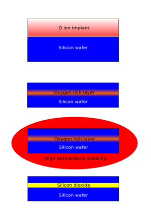
- SIMOX - Separation by IMplantation of OXygen – uses an oxygen ion beam implantation process followed by high temperature annealing to create a buried SiO2 layer.[13][14]
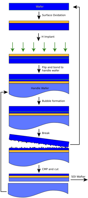
- Wafer bonding[15][16] – the insulating layer is formed by directly bonding oxidized silicon with a second substrate. The majority of the second substrate is subsequently removed, the remnants forming the topmost Si layer.
- One prominent example of a wafer bonding process is the Smart Cut method developed by the French firm Soitec which uses ion implantation followed by controlled exfoliation to determine the thickness of the uppermost silicon layer.
- NanoCleave is a technology developed by Silicon Genesis Corporation that separates the silicon via stress at the interface of silicon and silicon-germanium alloy.[17]
- ELTRAN is a technology developed by Canon which is based on porous silicon and water cut.[18]
- Seed methods[19] - wherein the topmost Si layer is grown directly on the insulator. Seed methods require some sort of template for homoepitaxy, which may be achieved by chemical treatment of the insulator, an appropriately oriented crystalline insulator, or vias through the insulator from the underlying substrate.
An exhaustive review of these various manufacturing processes may be found in reference[1]
Use in the microelectronics industry
IBM began to use SOI in the high-end RS64-IV "Istar" PowerPC-AS microprocessor in 2000. Other examples of microprocessors built on SOI technology include AMD's 130 nm, 90 nm, 65 nm, 45 nm and 32 nm single, dual, quad, six and eight core processors since 2001.[20] Freescale adopted SOI in their PowerPC 7455 CPU in late 2001, currently[when?] Freescale is shipping SOI products in 180 nm, 130 nm, 90 nm and 45 nm lines.[21] The 90 nm PowerPC- and Power ISA-based processors used in the Xbox 360, PlayStation 3, and Wii use SOI technology as well. Competitive offerings from Intel however continue[when?] to use conventional bulk CMOS technology for each process node, instead focusing on other venues such as HKMG and tri-gate transistors to improve transistor performance. In January 2005, Intel researchers reported on an experimental single-chip silicon rib waveguide Raman laser built using SOI.[22]
As for the traditional foundries, on July 2006 TSMC claimed no customer wanted SOI,[23] but Chartered Semiconductor devoted a whole fab to SOI.[24]
Use in high-performance radio frequency (RF) applications
In 1990, Peregrine Semiconductor began development of an SOI process technology utilizing a standard 0.5 μm CMOS node and an enhanced sapphire substrate. Its patented silicon on sapphire (SOS) process is widely used in high-performance RF applications. The intrinsic benefits of the insulating sapphire substrate allow for high isolation, high linearity and electro-static discharge (ESD) tolerance. Multiple other companies have also applied SOI technology to successful RF applications in smartphones and cellular radios.[25][additional citation(s) needed]
Use in photonics
SOI wafers are widely used in silicon photonics.[26] The crystalline silicon layer on insulator can be used to fabricate optical waveguides and other optical devices, either passive or active (e.g. through suitable implantations). The buried insulator enables propagation of infrared light in the silicon layer on the basis of total internal reflection. The top surface of the waveguides can be either left uncovered and exposed to air (e.g. for sensing applications), or covered with a cladding, typically made of silica[27]
Disadvantages
The major disadvantage of SOI technology when compared to conventional semiconductor industry is increased cost of manufacturing.[28] As of 2012 only IBM and AMD used SOI as basis for high-performance processors and the other manufacturers (Intel, TSMC, Global Foundries etc.) used conventional silicon wafers to build their CMOS chips.[28]
SOI market
As of 2020 the market utilizing the SOI process was projected to grow up by ~15% for the next 5 years according to Market Research Future group.[29]
See also
- Intel TeraHertz - similar technology from Intel
- Strain engineering
- Wafer (electronics)
- Wafer bonding
References
- ↑ 1.0 1.1 Celler, G. K.; Cristoloveanu, S. (2003). "Frontiers of silicon-on-insulator". Journal of Applied Physics 93 (9): 4955. doi:10.1063/1.1558223. Bibcode: 2003JAP....93.4955C.
- ↑ Marshall, Andrew; Natarajan, Sreedhar (2002). SOI design: analog, memory and digital techniques. Kluwer. ISBN 0-7923-7640-4.
- ↑ Colinge, Jean-Pierre (1991). Silicon-on-Insulator Technology: Materials to VLSI. Springer. ISBN 978-0-7923-9150-0.
- ↑ Mendez, Horacio (April 2009). "Silicon-on-insulator — SOI technology and ecosystem — Emerging SOI applications". SOI Industry Consortium. http://www.soiconsortium.org/pdf/Consortium_9april09_final.pdf.
- ↑ Kodeti, Narayan M. (October 2010). "Silicon On Insulator (SOI) Implementation". White Paper. Infotech. http://www.infotech-enterprises.com/fileadmin/infotech-enterprises.com/assets/downloads/White_Papers/Infotech_SOI_Paper_Oct_2010.pdf.
- ↑ "IBM touts chipmaking technology". 29 March 2001. https://www.cnet.com/news/ibm-touts-chipmaking-technology/.
- ↑ "SOI wafers with 30-100 Ang. Buried OX created by wafer bonding using 30-100 Ang. thin oxide as bonding layer" US patent 6835633
- ↑ "Ultra-thin body super-steep retrograde well (SSRW) FET devices" US patent 7002214
- ↑ Yang-Kyu Choi; Asano, K.; Lindert, N.; Subramanian, V.; Tsu-Jae King; Bokor, J.; Chenming Hu (May 2000). "Ultrathin-body SOI MOSFET for deep-sub-tenth micron era". IEEE Electron Device Letters 21 (5): 254–5. doi:10.1109/IEDM.1999.824298. http://www-device.eecs.berkeley.edu/~viveks/Papers/254EDL21.pdf.
- ↑ "Vertical MOSFET SRAM cell" US patent 7138685 describes SOI buried oxide (BOX) structures and methods for implementing enhanced SOI BOX structures
- ↑ Balestra, F. (1985). Characterization and Simulation of SOI MOSFETs with Back Potential Control (PhD). INP-Grenoble.
- ↑ Balestra, F. (2016). "1.5 Challenges to Ultralow-Power Semiconductor Device Operation". in Lury, S.; Xu, J.; Zaslavsky, A.. Future Trends in Microelectronics—Journey into the unknown. Wiley. pp. 69–81. doi:10.1002/9781119069225.ch1-5. ISBN 978-1-119-06922-5. https://books.google.com/books?id=FPnoDAAAQBAJ&pg=PA69.
- ↑ Atsushi Ogura, "Method of fabricating SOI substrate", US patent 5888297, issued 1999-03-30
- ↑ Hiroshi Fujioka, "Method of manufacturing semiconductor on insulator", US patent 5061642, issued 1991-10-29
- ↑ Tong, Q.-Y.; Gösele, U. (1998). SemiConductor Wafer Bonding: Science and Technology. Wiley. ISBN 978-0-471-57481-1.
- ↑ Bajor, George & et al., "Using a rapid thermal process for manufacturing a wafer bonded soi semiconductor", US patent 4771016, issued 1988-09-13
- ↑ "SIGEN.COM". http://www.sigen.com/.
- ↑ Yonehara, T; Sakaguchi, K.. "ELTRAN® Novel SOI Wafer Technology". Cutting Edge 2. Canon. http://www.jsapi.jsap.or.jp/Pdf/Number04/CuttingEdge2.pdf.
- ↑ US patent 5417180
- ↑ Vries, Hans de. "Chip Architect: Intel and Motorola/AMD's 130 nm processes to be revealed.". http://chip-architect.com/news/2000_11_07_process_130_nm.html.
- ↑ "NXP Semiconductors - Automotive, Security, IoT". http://www.freescale.com/webapp/sps/site/overview.jsp?nodeId=0121000303#soi.
- ↑ Rong, Haisheng; Liu, Ansheng; Jones, Richard; Cohen, Oded; Hak, Dani; Nicolaescu, Remus; Fang, Alexander; Paniccia, Mario (January 2005). "An all-silicon Raman laser". Nature 433 (7042): 292–4. doi:10.1038/nature03723. PMID 15931210. http://www.ece.ucsb.edu/uoeg/publications/papers/Rong05nature.pdf.
- ↑ "TSMC has no customer demand for SOI technology". Fabtech: The online information source for semiconductor professionals. http://www.fabtech.org/content/view/1698/74/.
- ↑ Chartered expands foundry market access to IBM's 90nm SOI technology
- ↑ Madden, Joe. "Handset RFFEs: MMPAs, Envelope Tracking, Antenna Tuning, FEMs, and MIMO". Mobile Experts. http://mobile-experts.net/manuals/mexp-rffe-12%20toc.pdf.
- ↑ Reed, Graham T.; Knights, Andrew P. (5 March 2004). Silicon Photonics: An Introduction. Wiley. ISBN 978-0-470-87034-1. https://books.google.com/books?id=6lsVVvFCBeAC&q=SOI+Wafers+in+Photonics&pg=PA111. Retrieved 22 April 2018.
- ↑ Rigny, Arnaud. "Silicon-on-Insulator Substrates: The Basis of Silicon Photonics". https://www.photonics.com/Articles/Silicon-on-Insulator_Substrates_The_Basis_of/a63021.
- ↑ 28.0 28.1 McLellan, Paul. "Silicon on Insulator (SOI)" (in en-US). https://semiwiki.com/semiconductor-services/1470-silicon-on-insulator-soi/.
- ↑ Future, Market Research (2021-02-17). "Silicon on Insulator (SoI) Market is Anticipated to Surpass USD 2.40 Billion By 2026 | APAC Region to Remain Forerunner in Global Silicon on Insulator Industry". GlobeNewswire News Room (Press release). Retrieved 2021-03-07.
External links
- SOI Industry Consortium - a site with extensive information and education for SOI technology
- SOI IP portal - A search engine for SOI IP
- AMDboard - a site with extensive information regarding SOI technology
- Advanced Substrate News - a newsletter about the SOI industry, produced by Soitec
- MIGAS '04 - The 7th session of MIGAS International Summer School on Advanced Microelectronics, devoted to SOI technology and devices
- MIGAS '09 - 12th session of the International Summer School on Advanced Microelectronics: "Silicon on Insulator (SOI) Nanodevices"
 |


