What is a simulation-based design of a semiconductor cleanroom?
February 4, 2024 - Reading time: 11 minutes
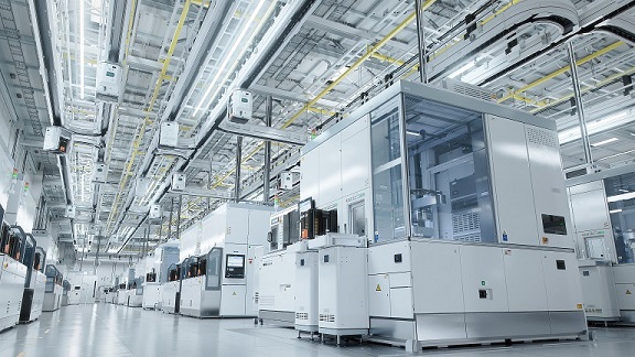
Design of Semiconductor Cleanroom
Designing a high-tech semiconductor cleanroom is no small feat - it requires extensive planning and an understanding of complex engineering principles. A well-designed semiconductor cleanroom ensures quality, safety and efficiency throughout the facility operations life.
Currently, the design of a semiconductor cleanroom is commonly based on a prescriptive approach which involves adopting a set design heuristic in the form of tables and charts. The prescriptive approach, which aims to cover as many building features, sizes, shapes and scenarios as possible, may lead to under- or over-estimation.
In contrast, simulation technology offers bespoke assessments specific to a building's features or scenarios and delivers much more accurate results than those relying on the prescriptive approach. This article aims to outline how simulation technology adds value to the design of a semiconductor cleanroom.
What Is a Semiconductor Cleanroom?
A semiconductor cleanroom is a specialized facility that maintains extremely low levels of airborne particles and other contaminants. Semiconductor cleanrooms are used in the manufacturing of integrated circuits, microchips and other semiconductor devices. In a well-designed semiconductor cleanroom, the concentration of airborne particles is controlled and maintained at very low levels using a combination of air filtration, airflow control and strict cleanliness protocols.
The cleanroom environment is designed to prevent the introduction of contaminants such as dust, moisture and organic compounds, which could interfere with the performance of the semiconductor devices being manufactured. Semiconductor cleanrooms are classified based on the maximum allowable concentration of particles of a specific size per unit of air volume. The most common classification system is the ISO 14644-1 standard, which defines various cleanroom classes ranging from ISO Class 1 (the cleanest) to ISO Class 9 (the least clean). The design and operation of a semiconductor cleanroom are highly specialized and require careful attention to detail to ensure the cleanliness and purity of the environment. Cleanroom personnel must follow strict protocols for gowning, cleaning and handling materials and equipment to minimize the risk of product contamination.
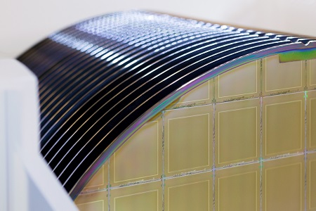
Microchip Wafers
Importance of Semiconductor Cleanroom
A semiconductor cleanroom provides the best environment for safe and efficient semiconductor manufacturing activities. The advantages of having a semiconductor cleanroom are:
- Minimizing the risk of particles, dust and other contaminants reaching sensitive components
- Ensuring high levels of air filtration to prevent airborne particles from impacting product quality
- Providing a temperature and humidity-controlled environment for consistent and reliable production results
- Creating an efficient workspace that promotes employee productivity and safety
- Providing safer work conditions that reduce potential health risks
- Creating products with consistent quality
Applications of CFD in a Semiconductor Cleanroom
There are several ways in which CFD simulation technology can be employed during the design stage of a semiconductor cleanroom. One of them is computational fluid dynamics (CFD), the science of predicting air flow, heat transfer and mass transfer by solving the mathematical equations that govern these processes using a numerical process. The following are examples of how CFD technology is applied during the design stage of a semiconductor cleanroom.
Air and Particles
At the design stage, CFD simulations can be used to model the flow of air and particles within the cleanroom, including the behavior of turbulence and the deposition or re-suspension of particles. Airflow dynamics inside a semiconductor cleanroom must be carefully controlled to ensure the removal of dust and other particles from the air. In addition, the airflow must be directed away from work surfaces and processing areas to minimize contamination. So, a well-designed system should also provide proper air circulation and ventilation. Vertical laminar top-to-bottom flow systems are commonly adopted in semiconductor cleanrooms. The air passing through the fan filter unit (FFU) traverses from the FFU surface downward and passes through the perforated flow before emerging on the chase side and returning to the dry cooling coil (DCC). Such an airflow profile with minimal recirculation flow helps maintain a clean environment by preventing dust accumulation and other contaminants. By analyzing the simulation results, designers can identify potential areas of particle accumulation and turbulence, optimize the cleanroom layout, air distribution system and air filtration to improve the overall cleanliness of the environment.
Temperature & Humidity
Maintaining consistent temperature and humidity levels ensures accurate and reliable results. Temperature and humidity control systems must be designed and calibrated to maintain these levels within the cleanroom environment. So, using the right sensors, controllers and other necessary equipment is important for efficient operation. The optimal temperature range for a semiconductor cleanroom is typically between 20°C and 24°C, whilst the humidity level should be between 40% and 60%. Controlling the temperature and humidity in a semiconductor cleanroom is critical for maintaining the quality and consistency of semiconductor manufacturing processes. This is because the physical and electrical properties of semiconductor materials are highly susceptible to changes in temperature and humidity, so even minor deviations from the required conditions can cause defects in the final product. Moisture can also cause particle agglomeration and increase the risk of particle contamination, which can negatively impact the quality of the semiconductor devices.
CFD can be used to simulate the temperature and humidity distribution within a semiconductor cleanroom. This helps to optimize the design of the cleanroom and its environmental control systems to ensure that the temperature and humidity levels are maintained within the specified range. CFD simulations can be used to evaluate different HVAC systems' performance and optimize the placement and design of air supply and exhaust vents. This helps ensure that the cleanroom airflow is properly distributed to maintain uniform temperature and humidity levels throughout the workspace. CFD simulations can also be used to analyze the impact of different environmental conditions on the cleanroom's performance. For example, simulations can be used to evaluate the effect of changes in external temperature and humidity levels on the internal cleanroom environment and to identify potential areas of temperature or humidity stratification. By analyzing the results of CFD simulations, designers can identify potential areas of temperature and humidity variation within the cleanroom and optimize the design of the environmental control systems to ensure that the temperature and humidity levels are maintained within the required range. This can help improve the quality and consistency of the semiconductor manufacturing process and reduce the risk of defects in the final products.
Smoke
CFD can be used to simulate the propagation of smoke in a semiconductor cleanroom in the event of a fire breakout. The CFD simulation provides valuable insight into the potential spread of smoke and can help optimize the design of a smoke evacuation system to ensure personnel safety. To simulate smoke propagation in a semiconductor cleanroom, a CFD model is developed that includes a realistic geometry of the cleanroom, the location and the size of the simulated fire source. The model also consists of the locations and flow rates of make-up air (MUA) vents, all the exhaust vents and smoke evacuation vents, commonly known in the industry as De-smoke units. Once the model is set up, it can be used to simulate the behavior of smoke in the cleanroom environment. The simulation can predict the concentration and propagation smoke throughout the cleanroom. Using these simulations, designers can identify potential areas of smoke accumulation and evaluate the effectiveness of different smoke management strategies. For example, they can test the efficacy of De-smoke units and the placement of exhaust vents to ensure that smoke is effectively restrained and/or evacuated from the cleanroom.
Other Simulation Technologies
Apart from simulating airflow profile, particles, temperature, humidity and smoke propagation using CFD, other simulation technologies add value during the design stage of a semiconductor cleanroom. For examples:
Water Hammer
A water hammer is a hydraulic phenomenon that occurs when a fluid in motion is suddenly stopped or redirected, creating a pressure surge or shock wave that can damage pipes, valves and other pipe fittings. Water hammer simulation can be used to predict and analyze water hammer in a fluid system and allow designers to optimize the system to minimize the risk of damage.
To simulate a water hammer, a virtual model of the fluid system is developed that includes the geometry of the pipes and components, the properties of the fluid such as density, viscosity, compressibility and boundary conditions such as flow rates and pressures. The model also includes valves, pumps, or other fittings that can affect fluid flow. Once the model is set up, it can be used to simulate the behavior of the fluid under different conditions, including sudden changes in flow or direction that can cause water hammer. The simulation can predict the pressure waves and resulting forces generated by the water hammer and the resulting stresses on the pipes and components. Using these simulations, designers can identify potential areas of risk for water hammer and optimize the design of the fluid system by mitigating the risk of damage. Water hammer simulation can also be used to test different scenarios and evaluate the effectiveness of various mitigation strategies, such as surge tanks, pressure relief valves and flow restrictors.
Pipe Stress Analysis
Pipe stress analysis is an important part of semiconductor cleanroom design, as the piping system must be designed to handle the pressures, temperatures and flow rates associated with the process equipment. The process of conducting pipe stress analysis in a semiconductor cleanroom design is similar to that of any other piping system but with some unique considerations due to the cleanroom environment. The first step in conducting pipe stress analysis is to create a 3D model of the piping system. Once the model is created, loads are applied to the system, including pressure, temperature, mass of the pipe and any associated equipment. In a semiconductor cleanroom, the loads may also include the vibration and movement of the process equipment. The analysis considers the material properties of the pipe and any support or other components, as well as the boundary conditions, such as the location and type of supports.
With the loads defined, the simulation results will determine the stresses and strains in the pipes and associated components and determine whether the stresses and strains in the system are within acceptable limits. If not, adjustments can be made to the system design, such as adding additional supports or modifying the piping layout. In a semiconductor cleanroom design, some unique considerations must be taken into account when conducting pipe stress analysis. For example, the piping system must be designed to minimize the risk of contamination, so materials and components that are compatible with the cleanroom environment must be used. The piping layout must also be optimized to minimize the number of connections and potential leakage points.
Process Cooling Water
Process cooling water (PCW) analysis is an important part of semiconductor cleanroom design, as the cooling water system is critical to maintaining the correct temperatures and pressures in the process equipment. The 3D model of the PCW system is created, taking into account the cooling water piping geometry, pumps, heat exchangers and other components. Once the model is created, boundary conditions such as the flow rates and pressures of the cooling water are defined. Simulation results will reveal the temperatures and flow rates of the cooling water throughout the system. The analysis considers the heat transfer characteristics of the process equipment and any associated heat exchangers, as well as the material properties of the piping and other components. Once the analysis is complete, the results are evaluated to determine whether the temperatures and pressures in the cooling water system are within acceptable limits. If they are not, adjustments can be made to the system design, such as adding additional chiller units, pumps and heat exchangers or modifying the piping layout.
Simulation technology adds value in the real-world semiconductor cleanroom design by ultimately confirming the effectiveness of a particular design or revealing design weaknesses before construction of the cleanroom begins thus reducing environmental impact by excluding unnecessary materials from the design. In addition, simulation technology also shortens the entire construction schedule by eliminating architectural design flaws and prevents their manifestation, all before construction begins.Overall, our end users were happy with the value added by simulation technology, which gave them a competitive edge over their competitors by leveraging shorter time to market.
Yap Wei Meng, Deputy Director, ASTI Pte Ltd
The examples outlined in this article on how simulation technologies add value during the design stage are the most common applications. There are also more unique applications of simulation technology employed during the design as well as the operations stage. Despite this, it is evident that simulation technology is a valuable tool that helps engineers working in the semiconductor industry to predict an event before it manifests itself. According to Yap Wei Meng, Deputy Director of ASTI Pte Ltd, a main contractor that has designed and built many semiconductor cleanrooms, simulation technology adds value in the real-world semiconductor cleanroom design by ultimately confirming the effectiveness of a particular design or revealing design weaknesses before construction of the cleanroom begins thus reducing environmental impact by excluding unnecessary materials from the design. In addition, simulation technology also shortens the entire construction schedule by eliminating architectural design flaws and prevents their manifestation, all before construction begins.
Overall, our end users were happy with the value added by simulation technology, which gave them a competitive edge over their competitors by leveraging shorter time to market.
Written by Jimmy Lea P/L
Engineering and Simulation Consultants