Engineering:DEC J-11
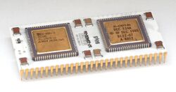
The J-11 is a microprocessor chip set that implements the PDP-11 instruction set architecture (ISA) jointly developed by Digital Equipment Corporation and Intersil. It was a high-end chip set designed to integrate the performance and features of the PDP-11/70 onto a handful of chips. It was used in the PDP-11/73, PDP-11/83 and Professional 380.
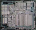
It consisted of a data path chip[1] and a control chip[2] in ceramic leadless packages mounted on a single ceramic hybrid DIP package. The control chip incorporated a control sequencer and a microcode ROM.[2] An optional separate floating-point accelerator (FPA) chip could be used, and was packaged in a standard DIP. The data path chip and control chip were fabricated by Intersil in a CMOS process while the FPA was fabricated by Digital in their "ZMOS" NMOS process.
The design originally was intended to support multiple control chips to allow implementation of additional instructions such as the Commercial Instruction Set (CIS), but no such control chips were ever offered.
A clone of the J-11 was manufactured in the Soviet Union under the designation KN1831VM1 (Russian: КН1831ВМ1).[3]
References
- ↑ "J-11 Data Chip Specification". Digital Equipment Corporation. July 1, 1982. http://www.bitsavers.org/pdf/dec/pdp11/j11/J-11_Data_Chip_Specification_Jul82.pdf.
- ↑ 2.0 2.1 "J-11 Control Chip Specification". Digital Equipment Corporation. June 22, 1982. http://www.bitsavers.org/pdf/dec/pdp11/j11/J-11_Control_Chip_Specification_Jun82.pdf.
- ↑ "Soviet microprocessors, microcontrollers, FPU chips and their western analogs". CPU-world. http://www.cpu-world.com/info/exUSSR-chips.html. Retrieved 24 March 2016.
 |


