Engineering:Delay-locked loop
In electronics, a delay-locked loop (DLL) is a pseudo-digital circuit similar to a phase-locked loop (PLL), with the main difference being the absence of an internal voltage-controlled oscillator, replaced by a delay line.
A DLL can be used to change the phase of a clock signal (a signal with a periodic waveform), usually to enhance the clock rise-to-data output valid timing characteristics of integrated circuits (such as DRAM devices). DLLs can also be used for clock recovery (CDR). From the outside, a DLL can be seen as a negative delay gate placed in the clock path of a digital circuit.
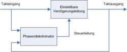
The main component of a DLL is a delay chain composed of many delay gates connected output-to-input. The input of the chain (and thus of the DLL) is connected to the clock that is to be negatively delayed. A multiplexer is connected to each stage of the delay chain; a control circuit automatically updates the selector of this multiplexer to produce the negative delay effect. The output of the DLL is the resulting, negatively delayed clock signal.
Another way to view the difference between a DLL and a PLL is that a DLL uses a variable phase (=delay) block, whereas a PLL uses a variable frequency block.
A DLL compares the phase of its last output with the input clock to generate an error signal which is then integrated and fed back as the control to all of the delay elements. The integration allows the error to go to zero while keeping the control signal, and thus the delays, where they need to be for phase lock. Since the control signal directly impacts the phase this is all that is required.
A PLL compares the phase of its oscillator with the incoming signal to generate an error signal which is then integrated to create a control signal for the voltage-controlled oscillator. The control signal impacts the oscillator's frequency, and phase is the integral of frequency, so a second integration is unavoidably performed by the oscillator itself.
In the Control Systems jargon, the DLL is a loop one step lower in order and in type with respect to the PLL, because it lacks the 1/s factor in the controlled block: the delay line has a transfer function phase-out/phase-in that is just a constant, the VCO transfer function is instead GVCO/s. In the comparison made in the previous sentences (that correspond to the figure where the integrator, and not the flat gain, is used), the DLL is a loop of 1st order and type 1 and the PLL of 2nd order and type 2. Without the integration of the error signal, the DLL would be 0th order and type 0, and the PLL 1st order and type 1.
The number of elements in the delay chain must be even, or else the duty cycle of the clock at the intermediate nodes of the chain might become irregular.
If 2N +1 was the -odd- number of stages, a 50% duty-cycle would become at times N/(2N+1), at times (N+1)/(2N+1), following the jittering of the error signal around the value corresponding to perfect lock.
Calling 2N the number of stages of the DLL chain, it is easy to see that the figure above would change from a DLL to a PLL, locked to the same phase and frequency, if the following modifications were made:
- dividing by two the number of stages
- making one of the stages an inverting one
- connecting the input of the chain of stages to its output instead of to the reference clock.
The resulting chain becomes a ring oscillator with a period equal to the delay of the previous chain, and the loop locks to the same reference clock with the same level of error signal.
The loop order and type are both incremented by one. It may be further remarked that, in the case where the integrator instead of the flat gain is chosen, the PLL that can be obtained is unstable.
The phase shift can be specified either in absolute terms (in delay chain gate units), or as a proportion of the clock period, or both.
See also
- Phase-locked loop (PLL)
- Digital Clock Manager (DCM)
- Clock signal
References
The Delay Lock Loop has been derived by J.J. Spilker, JR. and D.T. Magill, "The delay-lock discriminator--an optimum tracking device," Proc. IRE, vol.49, pp. 1403–1416, September 1961.
 |


