Physics:Smart cut
Smart cut is a technological process that enables the transfer of very fine layers of crystalline silicon material onto a mechanical support. It was invented by Michel Bruel of CEA-Leti, and was protected by US patent 5374564.[1] The application of this technological procedure is mainly in the production of silicon-on-insulator (SOI) wafer substrates.
The role of SOI is to electronically insulate a fine layer of monocrystalline silicon from the rest of the silicon wafer; an ultra-thin silicon film is transferred to a mechanical support, thereby introducing an intermediate, insulating layer. Semiconductor manufacturers can then fabricate integrated circuits on the top layer of the SOI wafers using the same processes they would use on plain silicon wafers.
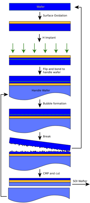
The sequence of illustrations pictorially describes the process involved in fabricating SOI wafers using the smart cut technology.
References
- ↑ Bruel, Michel, "Process for the production of thin semiconductor material films", US patent 5374564, published 20 December 1994
See also
- Silicon on insulator
- Soitec
- CEA-Leti
 |


