Physics:Bridgman–Stockbarger technique
The Bridgman–Stockbarger technique is named after Harvard physicist Percy Williams Bridgman (1882-1961) and MIT physicist Donald C. Stockbarger (1895–1952). The technique includes two similar but distinct methods primarily used for growing boules (single crystal ingots), but which can be used for solidifying polycrystalline ingots as well.
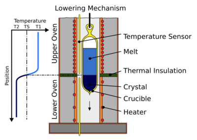
The methods involve heating polycrystalline material above its melting point and slowly cooling it from one end of its container, where a seed crystal is located. A single crystal of the same crystallographic orientation as the seed material is grown on the seed and is progressively formed along the length of the container. The process can be carried out in a horizontal or vertical orientation, and usually involves a rotating crucible/ampoule to stir the melt.[1]
The Bridgman method is a popular way of producing certain semiconductor crystals such as gallium arsenide, for which the Czochralski process is more difficult. The process can reliably produce single crystal ingots, but does not necessarily result in uniform properties through the crystal.[1]
The difference between the Bridgman[2] technique and Stockbarger[3] technique is subtle: While both methods utilize a temperature gradient and a moving crucible, the Bridgman technique utilizes the relatively uncontrolled gradient produced at the exit of the furnace; the Stockbarger technique introduces a baffle, or shelf, separating two coupled furnaces with temperatures above and below the freezing point. Stockbarger's modification of the Bridgman technique allows for better control over the temperature gradient at the melt/crystal interface.
When seed crystals are not employed as described above, polycrystalline ingots can be produced from a feedstock consisting of rods, chunks, or any irregularly shaped pieces once they are melted and allowed to re-solidify. The resultant microstructure of the ingots so obtained are characteristic of directionally solidified metals and alloys with their aligned grains.
A variant of the technique known as the horizontal directional solidification method or HDSM developed by Khachik Bagdasarov starting in the 1960s in the Soviet Union uses a flat-bottomed crucible with short sidewalls rather than an enclosed ampoule, and has been used to grow various large oxide crystals including Yb:YAG (a laser host crystal),[4] and sapphire crystals 45 cm wide and over 1 meter long.[5]
See also
References
- ↑ Jump up to: 1.0 1.1 Hans J. Scheel; Peter Capper; Peter Rudolph (25 October 2010). Crystal Growth Technology: Semiconductors and Dielectrics. John Wiley & Sons. pp. 177–178. ISBN 978-3-527-32593-1. https://books.google.com/books?id=Jq9t9QE0LNwC&pg=PA177.
- ↑ Bridgman, Percy W. (1925). "Certain Physical Properties of Single Crystals of Tungsten, Antimony, Bismuth, Tellurium, Cadmium, Zinc, and Tin". Proceedings of the American Academy of Arts and Sciences 60 (6): 305–383. doi:10.2307/25130058.
- ↑ Stockbarger, Donald C. (1936). "The Production of Large Single Crystals of Lithium Fluoride". Review of Scientific Instruments 7 (3): 133–136. doi:10.1063/1.1752094. Bibcode: 1936RScI....7..133S.
- ↑ Arzakantsyan, M.; Ananyan, N.; Gevorgyan, V.; Chanteloup, J.-C. (2012). "Growth of large 90 mm diameter Yb:YAG single crystals with Bagdasarov method". Optical Materials Express 2 (9): 1219–1225. doi:10.1364/OME.2.001219.
- ↑ Montgomery, Matthew; Blockburger, Clark (2017). Zelinski, Brian J.. ed. "18 x 36 x 1.5 inch sapphire panels for visible and infrared windows". Proc. SPIE. Window and Dome Technologies and Materials XV 10179 101790N-1 (Window and Dome Technologies and Materials XV): 101790N. doi:10.1117/12.2269465.


