Engineering:Frequency compensation
In electronics engineering, frequency compensation is a technique used in amplifiers, and especially in amplifiers employing negative feedback. It usually has two primary goals: To avoid the unintentional creation of positive feedback, which will cause the amplifier to oscillate, and to control overshoot and ringing in the amplifier's step response. It is also used extensively to improve the bandwidth of single pole systems.
Explanation
Most amplifiers use negative feedback to trade gain for other desirable properties, such as decreased distortion, improved noise reduction or increased invariance to variation of parameters such as temperature. Ideally, the phase characteristic of an amplifier's frequency response would be linear; however, device limitations make this goal physically unattainable. More particularly, capacitances within the amplifier's gain stages cause the output signal to lag behind the input signal by up to 90° for each pole they create.[lower-alpha 1] If the sum of these phase lags reaches 180°, the output signal will be the negative of the input signal. Feeding back any portion of this output signal to the inverting (negative) input when the gain of the amplifier is sufficient will cause the amplifier to oscillate. This is because the feedback signal will reinforce the input signal. That is, the feedback is then positive rather than negative.
Frequency compensation is implemented to avoid this result.
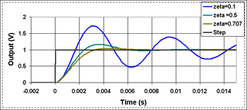
Another goal of frequency compensation is to control the step response of an amplifier circuit as shown in Figure 1. For example, if a step in voltage is input to a voltage amplifier, ideally a step in output voltage would occur. However, the output is not ideal because of the frequency response of the amplifier, and ringing occurs. Several figures of merit to describe the adequacy of step response are in common use. One is the rise time of the output, which ideally would be short. A second is the time for the output to lock into its final value, which again should be short. The success in reaching this lock-in at final value is described by overshoot (how far the response exceeds final value) and settling time (how long the output swings back and forth about its final value). These various measures of the step response usually conflict with one another, requiring optimization methods.
Frequency compensation is implemented to optimize step response, one method being pole splitting.A
Use in operational amplifiers
Because operational amplifiers are so ubiquitous and are designed to be used with feedback, the following discussion will be limited to frequency compensation of these devices.
It should be expected that the outputs of even the simplest operational amplifiers will have at least two poles. A consequence of this is that at some critical frequency, the phase of the amplifier's output = −180° compared to the phase of its input signal. The amplifier will oscillate if it has a gain of one or more at this critical frequency. This is because (a) the feedback is implemented through the use of an inverting input that adds an additional −180° to the output phase making the total phase shift −360° and (b) the gain is sufficient to induce oscillation.
A more precise statement of this is the following: An operational amplifier will oscillate at the frequency at which its open loop gain equals its closed loop gain if, at that frequency,
- The open loop gain of the amplifier is ≥ 1 and
- The difference between the phase of the open loop signal and phase response of the network creating the closed loop output = −180°. Mathematically: [math]\displaystyle{ \Phi_{OL} - \Phi_{CLnet} = -180^\circ }[/math]
Practice
Frequency compensation is implemented by modifying the gain and phase characteristics of the amplifier's open loop output or of its feedback network, or both, in such a way as to avoid the conditions leading to oscillation. This is usually done by the internal or external use of resistance-capacitance networks.
Dominant-pole compensation
The method most commonly used is called dominant-pole compensation, which is a form of lag compensation. It is an external compensation technique and is used for relatively low closed loop gain. A pole placed at an appropriate low frequency in the open-loop response reduces the gain of the amplifier to one (0 dB) for a frequency at or just below the location of the next highest frequency pole. The lowest frequency pole is called the dominant pole because it dominates the effect of all of the higher frequency poles. The result is that the difference between the open loop output phase and the phase response of a feedback network having no reactive elements never falls below −180° while the amplifier has a gain of one or more, ensuring stability.
Dominant-pole compensation can be implemented for general purpose operational amplifiers by adding an integrating capacitance to the stage that provides the bulk of the amplifier's gain. This capacitor creates a pole that is set at a frequency low enough to reduce the gain to one (0 dB) at or just below the frequency where the pole next highest in frequency is located. The result is a phase margin of ≈ 45°, depending on the proximity of still higher poles.[lower-alpha 2] This margin is sufficient to prevent oscillation in the most commonly used feedback configurations. In addition, dominant-pole compensation allows control of overshoot and ringing in the amplifier step response, which can be a more demanding requirement than the simple need for stability.
This compensation method is described below: Let [math]\displaystyle{ A }[/math] be the uncompensated transfer function of op amp in open-loop configuration which is given by:
[math]\displaystyle{ A(s) = A_{OL}\cdot \frac{1}{1+\frac{s}{\omega_1}} \cdot \frac{1}{1+\frac{s}{\omega_2}} \cdot \frac{1}{1+\frac{s}{\omega_3}}= A_{OL}\cdot \frac{\omega_1\omega_2\omega_3}{(s+\omega1)(s+\omega_2)(s+\omega_3)} }[/math]
where [math]\displaystyle{ A_{OL} }[/math] is the open-loop gain of the Op-Amp and [math]\displaystyle{ \omega_1 }[/math], [math]\displaystyle{ \omega_2 }[/math], and [math]\displaystyle{ \omega_3 }[/math] are the angular frequencies at which the gain function [math]\displaystyle{ A(s) }[/math] rolls off by -20dB, -40dB, and -60dB respectively.
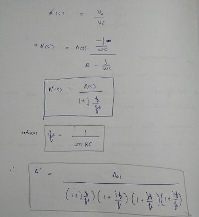
Thus, for compensation, introduce a dominant pole by adding an RC network in series with the Op-Amp as shown in the figure.
The Transfer function of the compensated open loop Op-Amp circuit is given by:
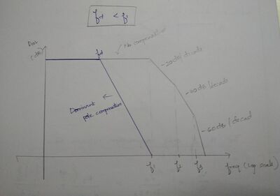
where fd < f1 < f2 < f3
The compensation capacitance C is chosen such that fd < f1. Hence, the frequency response of a dominant pole compensated open loop Op-Amp circuit shows uniform gain roll off from fd and becomes 0 at f1 as shown in the graph.
The advantages of dominant pole compensation are: 1. It is simple and effective. 2. Noise immunity is improved since noise frequency components outside the bandwidth are eliminated.
Though simple and effective, this kind of conservative dominant pole compensation has two drawbacks:
- It reduces the bandwidth of the amplifier, thereby reducing available open loop gain at higher frequencies. This, in turn, reduces the amount of feedback available for distortion correction, etc. at higher frequencies.
- It reduces the amplifier's slew rate. This reduction results from the time it takes the finite current driving the compensated stage to charge the compensating capacitor. The result is the inability of the amplifier to reproduce high amplitude, rapidly changing signals accurately.
Often, the implementation of dominant-pole compensation results in the phenomenon of Pole splitting. This results in the lowest frequency pole of the uncompensated amplifier "moving" to an even lower frequency to become the dominant pole, and the higher-frequency pole of the uncompensated amplifier "moving" to a higher frequency. To overcome these disadvantages, pole zero compensation is used.
Other methods
Some other compensation methods are: lead compensation, lead–lag compensation and feed-forward compensation.
- Lead compensation. Whereas dominant pole compensation places or moves poles in the open loop response, lead compensation places a zero[lower-alpha 3] in the open loop response to cancel one of the existing poles.
- Lead–lag compensation places both a zero and a pole in the open loop response, with the pole usually being at an open loop gain of less than one.
- Feed-forward or Miller compensation uses a capacitor to bypass a stage in the amplifier at high frequencies, thereby eliminating the pole that stage creates.
The purpose of these three methods is to allow greater open loop bandwidth while still maintaining amplifier closed loop stability. They are often used to compensate high gain, wide bandwidth amplifiers.
Footnotes
- ↑ In this context, a pole is the point in a frequency response curve where the amplitude decreases by 3db due to an integrating resistance and capacitive reactance. Ultimately, each pole will result in a phase lag of up to 90°, i.e., the output signal will lag behind the input signal by 90° at this point. For the mathematical concept of a pole, see, Pole (complex analysis).
- ↑ The dominant pole produces a phase shift approximating −90° from approx. 10 times the pole frequency to a frequency a factor of ten below the next higher pole position. The next higher pole, in turn, adds another −45° for a frequency at its location for a total of −135° (neglecting the still higher poles).
- ↑ In this context, a zero is the point in a frequency response curve where the amplitude increases by 3db due to a differentiating resistance and capacitive reactance. Ultimately, each zero will result in a phase lead of 90°, i.e., the phase of the output signal will be 90° ahead of the phase of the input signal at this point. For the mathematical concept of a zero, see, Zero (complex analysis).
See also
- Pole splitting
- Bode plot
- Negative feedback amplifier
- Step response
 |


