Engineering:Capacitance–voltage profiling
Capacitance–voltage profiling (or C–V profiling, sometimes CV profiling) is a technique for characterizing semiconductor materials and devices. The applied voltage is varied, and the capacitance is measured and plotted as a function of voltage. The technique uses a metal–semiconductor junction (Schottky barrier) or a p–n junction[1] or a MOSFET to create a depletion region, a region which is empty of conducting electrons and holes, but may contain ionized donors and electrically active defects or traps. The depletion region with its ionized charges inside behaves like a capacitor. By varying the voltage applied to the junction it is possible to vary the depletion width. The dependence of the depletion width upon the applied voltage provides information on the semiconductor's internal characteristics, such as its doping profile and electrically active defect densities.[2], [3] Measurements may be done at DC, or using both DC and a small-signal AC signal (the conductance method [3], [4]), or using a large-signal transient voltage.[5]
Application
Many researchers use capacitance–voltage (C–V) testing to determine semiconductor parameters, particularly in MOSCAP and MOSFET structures. However, C–V measurements are also widely used to characterize other types of semiconductor devices and technologies, including bipolar junction transistors, JFETs, III–V compound devices, photovoltaic cells, MEMS devices, organic thin-film transistor (TFT) displays, photodiodes, and carbon nanotubes (CNTs).
These measurements' fundamental nature makes them applicable to a wide range of research tasks and disciplines. For example, researchers use them in university and semiconductor manufacturers' labs to evaluate new processes, materials, devices, and circuits. These measurements are extremely valuable to product and yield enhancement engineers who are responsible for improving processes and device performance. Reliability engineers also use these measurements to qualify the suppliers of the materials they use, to monitor process parameters, and to analyze failure mechanisms.
A multitude of semiconductor device and material parameters can be derived from C–V measurements with appropriate methodologies, instrumentation, and software. This information is used throughout the semiconductor production chain, and begins with evaluating epitaxially grown crystals, including parameters such as average doping concentration, doping profiles, and carrier lifetimes.
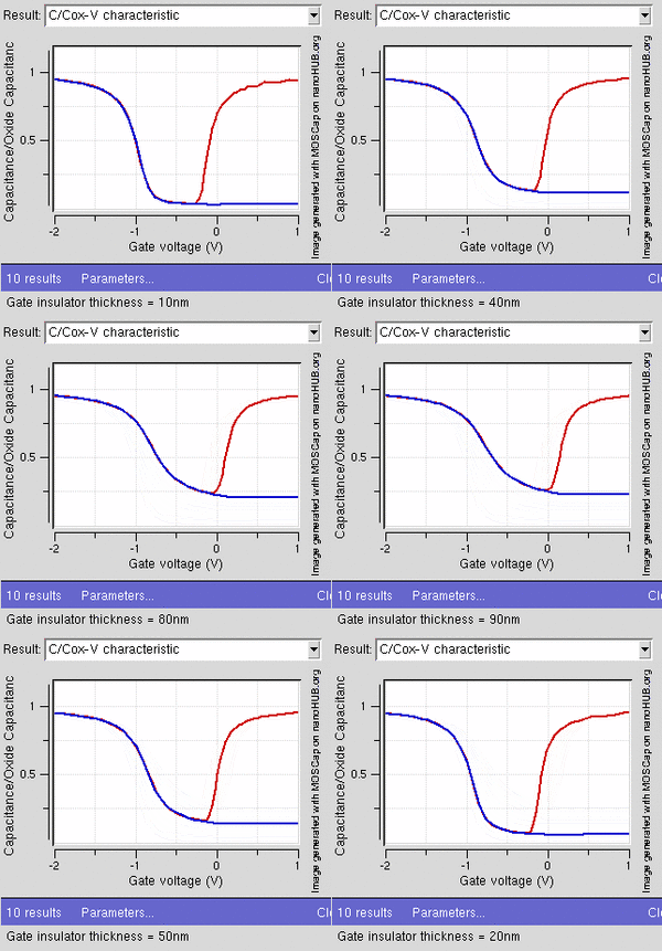
C–V measurements can reveal oxide thickness, oxide charges, contamination from mobile ions, and interface trap density in wafer processes. A C–V profile as generated on nanoHUB for bulk MOSFET with different oxide thicknesses. Notice that the red curve indicates low frequency whereas the blue curve illustrates the high-frequency C–V profile. Pay particular attention to the shift in threshold voltage with different oxide thicknesses.
These measurements continue to be important after other process steps have been performed, including lithography, etching, cleaning, dielectric and polysilicon depositions, and metallization, among others. Once devices have been fully fabricated, C–V profiling is often used to characterize threshold voltages and other parameters during reliability and basic device testing and to model device performance.
C–V measurements are done by using capacitance–voltage meters of Electronic Instrumentation. They are used to analyze the doping profiles of semiconductor devices by the obtained C–V graphs.
C–V characteristics of metal–oxide–semiconductor structure
A metal–oxide–semiconductor structure is critical part of a MOSFET, controlling the height of potential barrier in the channel via the gate oxide.
An n-channel MOSFET's operation can be divided into three regions, shown below and corresponding to the right figure.
Depletion
When a small positive bias voltage is applied to the metal, the valence band edge is driven far from the Fermi level, and holes from the body are driven away from the gate, resulting in a low carrier density, so the capacitance is low (the valley in the middle of the figure to the right).
Inversion
At larger gate bias still, near the semiconductor surface the conduction band edge is brought close to the Fermi level, populating the surface with electrons in an inversion layer or n-channel at the interface between the semiconductor and the oxide. This results in a capacitance increase, as shown in the right part of right figure.
Accumulation
When a negative gate-source voltage (positive source-gate) is applied, it creates a p-channel at the surface of the n region, analogous to the n-channel case, but with opposite polarities of charges and voltages. The increase in hole density corresponds to increase in capacitance, shown in the left part of right figure.
See also
- Current–voltage characteristic
- Depletion region
- Depletion width
- Drive Level Capacitance Profiling
- Deep-level transient spectroscopy
- Metal–oxide–semiconductor structure
References
- ↑ J. Hilibrand and R.D. Gold, "Determination of the Impurity Distribution in Junction Diodes From Capacitance-Voltage Measurements", RCA Review, vol. 21, p. 245, June 1960
- ↑ Alain C. Diebold, ed (2001). Handbook of Silicon Semiconductor Metrology. CRC Press. pp. 59–60. ISBN 0-8247-0506-8. https://books.google.com/books?id=9B7e7rNnZPcC&q=metrology+%22capacitance+voltage+%22&pg=PA59.
- ↑ 3.0 3.1 E.H. Nicollian, J.R. Brews (2002). MOS (Metal Oxide Semiconductor) Physics and Technology. Wiley. ISBN 978-0-471-43079-7. https://books.google.com/books?as_isbn=0-471-43079-X.
- ↑ Andrzej Jakubowski, Henryk M. Przewłocki (1991). Diagnostic Measurements in LSI/VLSI Integrated Circuits Production. World Scientific. p. 159. ISBN 981-02-0282-2. https://books.google.com/books?id=MfM3VtXhpRwC&q=conductance+method&pg=PA159.
- ↑ Sheng S. Li and Sorin Cristoloveanu (1995). Electrical Characterization of Silicon-On-Insulator Materials and Devices. Springer. pp. Chapter 6, p. 163. ISBN 0-7923-9548-4. https://books.google.com/books?id=AAr0_xwg9SgC&q=DLTS&pg=PA163.
External links
- MOScap simulator on nanoHUB.org enables users to compute C-V characteristics for different doping profiles, materials, and temperatures.
 |


