Multi-level cell
In electronics, a multi-level cell (MLC) is a memory cell capable of storing more than a single bit of information, compared to a single-level cell (SLC), which can store only one bit per memory cell. A memory cell typically consists of a single floating-gate MOSFET (metal–oxide–semiconductor field-effect transistor), thus multi-level cells reduce the number of MOSFETs required to store the same amount of data as single-level cells.
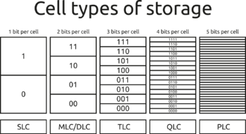
Triple-level cells (TLC) and quad-level cells (QLC) are versions of MLC memory, which can store three and four bits per cell respectively. The name "multi-level cell" is sometimes used specifically to refer to the "two-level cell". Overall, the memories are named as follows:
- Single-level cell or SLC (1 bit per cell)
- Multi-level cell or MLC (2 bits per cell), alternatively double-level cell or DLC
- Triple-level cell or TLC (3 bits per cell) or 3-Bit MLC
- Quad-level cell or QLC (4 bits per cell)
- Penta-level cell or PLC (5 bits per cell) – currently in development[1]
Notice that this nomenclature can be misleading, since an "n-level cell" in fact uses 2n levels of charge to store n bits (see below).
Typically, as the "level" count increases, performance (speed and reliability) and consumer cost decrease; however, this correlation can vary between manufacturers.
Examples of MLC memories are MLC NAND flash, MLC PCM (phase-change memory), etc. For example, in SLC NAND flash technology, each cell can exist in one of the two states, storing one bit of information per cell. Most MLC NAND flash memory has four possible states per cell, so it can store two bits of information per cell. This reduces the amount of margin separating the states and results in the possibility of more errors. Multi-level cells that are designed for low error rates are sometimes called enterprise MLC (eMLC).
New technologies, such as multi-level cells and 3D Flash, and increased production volumes will continue to bring prices down.[2]
Single-level cell
Flash memory stores data in individual memory cells, which are made of floating-gate MOSFET transistors. Traditionally, each cell had two possible states (each with one voltage level), with each state representing either a one or a zero, so one bit of data was stored in each cell in so-called single-level cells, or SLC flash memory. SLC memory has the advantage of higher write speeds, lower power consumption and higher cell endurance. However, because SLC memory stores less data per cell than MLC memory, it costs more per megabyte of storage to manufacture. Due to higher transfer speeds and expected longer life, SLC flash technology is used in high-performance memory cards. In February 2016, a study was published that showed little difference in practice between the reliability of SLC and MLC.[3]
A single-level cell (SLC) flash memory may have a lifetime of about 50,000 to 100,000 program/erase cycles.[4]
A single-level cell represents a 1 when almost empty and a 0 when almost full. There is a region of uncertainty (a read margin) between the two possible states at which the data stored in the cell cannot be precisely read.[5]
Multi-level cell
The primary benefit of MLC flash memory is its lower cost per unit of storage due to the higher data density, and memory-reading software can compensate for a larger bit error rate.[6] The higher error rate necessitates an error-correcting code (ECC) that can correct multiple bit errors; for example, the SandForce SF-2500 flash controller can correct up to 55 bits per 512-byte sector with an unrecoverable read error rate of less than one sector per 1017 bits read.[7] The most commonly used algorithm is Bose–Chaudhuri–Hocquenghem (BCH code).[8] Other drawbacks of MLC NAND are lower write speeds, lower number of program/erase cycles and higher power consumption compared to SLC flash memory.
Read speeds can also be lower for MLC NAND than SLC due to the need to read the same data at a second threshold voltage to help resolve errors. TLC and QLC devices may need to read the same data up to 4 and 8 times respectively to obtain values that are correctable by ECC.[9]
MLC flash may have a lifetime of about 1,000 to 10,000 program/erase cycles. This typically necessitates the use of a flash file system, which is designed around the limitations of flash memory, such as using wear leveling to extend the useful lifetime of the flash device.
The Intel 8087 used two-bits-per-cell technology for its microcode ROM,[10] and in 1980 was one of the first devices on the market to use multi-level ROM cells.[11][12] Intel later demonstrated 2-bit multi-level cell (MLC) NOR flash in 1997.[13] NEC demonstrated quad-level cells in 1996, with a 64 Mbit flash memory chip storing 2 bits per cell. In 1997, NEC demonstrated a dynamic random-access memory (DRAM) chip with quad-level cells, holding a capacity of 4 Gbit. STMicroelectronics also demonstrated quad-level cells in 2000, with a 64 Mbit NOR flash memory chip.[14]
MLC is used to refer to cells that store 2 bits per cell, using 4 charge values or levels. A 2-bit MLC has a single charge level assigned to every possible combination of ones and zeros, as follows: When close to 25% full, the cell represents a binary value of 11; when close to 50%, the cell represents a 01; when close to 75%, the cell represents a 00; and when close to 100%, the cell represents a 10. Once again, there is a region of uncertainty (read margin) between values, at which the data stored in the cell cannot be precisely read.[15][5]
(As of 2013) some solid-state drives use part of an MLC NAND die as if it were single-bit SLC NAND, giving higher write speeds.[16][17][18]
(As of 2018) nearly all commercial MLCs are planar-based (i.e. cells are built on silicon surface) and so subject to scaling limitations. To address this potential problem, the industry is already looking at technologies that can guarantee storage density increases beyond today’s limitations. One of the most promising is 3D Flash, where cells are stacked vertically, thereby avoiding the limitations of planar scaling.[19]
In the past, a few memory devices went the other direction and used two cells per bit to give even lower bit error rates.[20]
Enterprise MLC (eMLC) is a more expensive variant of MLC that is optimized for commercial use. It claims to last longer and be more reliable than normal MLCs while providing cost savings over traditional SLC drives. Although many SSD manufacturers have produced MLC drives intended for enterprise use, only Micron sells raw NAND Flash chips under this designation.[21]
Triple-level cell
A triple-level cell (TLC) is a type of NAND flash memory that stores 3 bits of information per cell. Toshiba introduced memory with triple-level cells in 2009.[22]
Samsung announced a type of NAND flash that stores 3 bits of information per cell, with 8 total voltage states (values or levels), coining the term "triple-level cell" ("TLC"). Samsung Electronics began mass-producing it in 2010,[23] and it was first seen in Samsung's 840 Series SSDs.[24] Samsung refers to this technology as 3-bit MLC. The negative aspects of MLC are amplified with TLC, but TLC benefits from still higher storage density and lower cost.[25]
In 2013, Samsung introduced V-NAND (Vertical NAND, also known as 3D NAND) with triple-level cells, which had a memory capacity of 128 Gbit.[26] They expanded their TLC V-NAND technology to 256 Gbit memory in 2015,[23] and 512 Gbit in 2017.[27]
Quad-level cell
Memory that stores 4 bits per cell is commonly referred to as quad-level cell (QLC), following the convention set by TLC. Prior to its invention, the term "QLC" was synonymous with MLC in referring to cells that can have 4 voltage states, i.e. ones that store 2 bits per cell – what is now unambiguously referred to as DLC.[citation needed]
In 2009, Toshiba and SanDisk introduced NAND flash memory chips with quad-level cells, storing 4 bits per cell and holding a capacity of 64 Gbit.[22][28]
SanDisk X4 flash memory cards, introduced in 2009, was one of the first products based on NAND memory that stores 4 bits per cell, commonly referred to as quad-level-cell (QLC), using 16 discrete charge levels (states) in each individual transistor. The QLC chips used in these memory cards were manufactured by Toshiba, SanDisk and SK Hynix.[29][30]
In 2017, Toshiba introduced V-NAND memory chips with quad-level cells, which have a storage capacity of up to 768 Gbit.[31] In 2018, ADATA, Intel, Micron and Samsung have launched some SSD products using QLC NAND memory.[32][33][34][35]
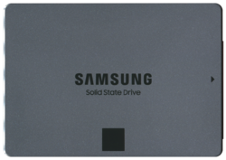
In 2020, Samsung released a QLC SSD with storage space up to 8 TB for customers. It is the SATA SSD with the largest storage capacity for end customers as of 2020.[36][37]
See also
References
- ↑ "Solidigm Demonstrates World's First Penta-Level Cell SSD at Flash Memory Summit" (in en). 2022-08-02. https://news.solidigm.com/en-WW/217006-solidigm-demonstrates-world-s-first-penta-level-cell-ssd-at-flash-memory-summit.
- ↑ "NAND Flash is Displacing Hard Disk Drives". https://www.hyperstone.com/en/NAND-Flash-is-displacing-hard-disk-drives-1249,12728.html.
- ↑ Bianca Schroeder and Arif Merchant (February 22, 2016). "Flash Reliability in Production: The Expected and the Unexpected". Conference on File and Storage Technologies (Usenix). ISBN 9781931971287. https://www.usenix.org/conference/fast16/technical-sessions/presentation/schroeder. Retrieved November 3, 2016.
- ↑ "Hyperstone Blog | NAND Flash is displacing hard disk drives" (in en). https://www.hyperstone.com/en/NAND-Flash-is-displacing-hard-disk-drives-1249.html.
- ↑ 5.0 5.1 Shimpi, Anand Lal. "The Intel SSD 710 (200GB) Review". https://www.anandtech.com/show/4902/intel-ssd-710-200gb-review.
- ↑ Micron's MLC NAND Flash Webinar. .
- ↑ "SandForce® SF2600 and SF2500 Enterprise datasheet". https://www.seagate.com/www-content/product-content/lsi-fam/enterprise-flash-controller/en-us/docs/enterprise-fsp-sf-2500-ds1828-1-1409us.pdf.
- ↑ EETimes (2013-08-27). "A Tour of the Basics of Embedded NAND Flash Options". https://www.eetimes.com/a-tour-of-the-basics-of-embedded-nand-flash-options/.
- ↑ Peleato (Sep 2015). "Adaptive Read Thresholds for NAND Flash". IEEE Transactions on Communications 63 (9): 3069–3081. doi:10.1109/TCOMM.2015.2453413.
- ↑ "Two bits per transistor: high-density ROM in Intel's 8087 floating point chip". http://www.righto.com/2018/09/two-bits-per-transistor-high-density.html.
- ↑ "Four-state cell called density key" article by J. Robert Lineback. "Electronics" magazine. 1982 June 30.
- ↑ P. Glenn Gulak (2018-05-28). "A Review of Multiple-Valued Memory Technology". Proceedings. 1998 28th IEEE International Symposium on Multiple- Valued Logic (Cat. No.98CB36138). pp. 222–231. doi:10.1109/ISMVL.1998.679447. ISBN 978-0-8186-8371-8. https://pdfs.semanticscholar.org/a3c1/cbc425c7987fe2307b48e0ff96f2c2c1b038.pdf. Retrieved 2023-02-11.
- ↑ "The Flash Memory Market". Smithsonian Institution. 1997. http://smithsonianchips.si.edu/ice/cd/MEMORY97/SEC05.PDF.
- ↑ "Memory". http://maltiel-consulting.com/Semiconductor_technology_memory.html.
- ↑ Pedro Hernandez (June 29, 2018). "SLC vs MLC vs TLC NAND Flash". https://www.enterprisestorageforum.com/storage-hardware/slc-vs-mlc-vs-tlc-nand-flash.html.
- ↑ Gasior, Geoff (2013-07-25). "Samsung's 840 EVO solid-state drive reviewed" (in en-US). https://techreport.com/review/25122/samsungs-840-evo-solid-state-drive-reviewed/.
- ↑ "New Samsung 840 EVO employs TLC and pseudo-SLC TurboWrite cache - PC Perspective" (in en-US). 2013-07-18. https://pcper.com/2013/07/new-samsung-840-evo-employs-tlc-and-pseudo-slc-turbowrite-cache/.
- ↑ Samsung. "Samsung Solid State Drive: TurboWrite Technology White Paper". 2013.
- ↑ "Hyperstone Blog | Solid State bit density and the Flash Memory Controller" (in en). 2018-04-17. https://www.hyperstone.com/en/Solid-State-bit-density-and-the-Flash-Memory-Controller-1235.html.
- ↑ Prophet, Graham (2008-10-02). "Automotive EEPROMs use two cells per bit for ruggedness, reliability" (in en-US). https://www.edn.com/automotive-eeproms-use-two-cells-per-bit-for-ruggedness-reliability/.
- ↑ "Enterprise MLC: Extended MLC Cycling Capabilities" (in en). https://www.micron.com/products/nand-flash/mlc-nand/enterprise-mlc.
- ↑ 22.0 22.1 "Toshiba Makes Major Advances in NAND Flash Memory with 3-bit-per-cell 32nm generation and with 4-bit-per-cell 43nm technology". Toshiba. 11 February 2009. http://www.toshiba.co.jp/about/press/2009_02/pr1102.htm.
- ↑ 23.0 23.1 "History". Samsung. https://www.samsung.com/us/aboutsamsung/company/history/.
- ↑ "Samsung SSD 840 Series – 3BIT/MLC NAND Flash". http://www.samsung.com/global/business/semiconductor/minisite/SSD/uk/html/about/MlcNandFlash.html.
- ↑ "Samsung SSD 840: Testing the Endurance of TLC NAND". AnandTech. 2012-11-16. http://www.anandtech.com/show/6459/samsung-ssd-840-testing-the-endurance-of-tlc-nand.
- ↑ "Samsung Mass Producing 128Gb 3-bit MLC NAND Flash". Tom's Hardware. 11 April 2013. https://www.tomshardware.co.uk/NAND-128Gb-Mass-Production-3-bit-MLC,news-43458.html.
- ↑ Shilov, Anton (December 5, 2017). "Samsung Starts Production of 512 GB UFS NAND Flash Memory: 64-Layer V-NAND, 860 MB/s Reads". AnandTech. https://www.anandtech.com/show/12120/samsung-starts-production-of-512-gb-ufs-chips.
- ↑ "SanDisk ships world's first memory cards with 64 gigabit X4 NAND flash". SlashGear. 13 October 2009. https://www.slashgear.com/sandisk-ships-worlds-first-memory-cards-with-64-gigabit-x4-nand-flash-1360217/.
- ↑ McGlaun, Shane (2009-10-13). "SanDisk Ships World's First Memory Cards With 64 Gigabit X4 NAND Flash" (in en-US). https://www.slashgear.com/sandisk-ships-worlds-first-memory-cards-with-64-gigabit-x4-nand-flash-1360217/.
- ↑ Choi, Young (2009-05-05). "NAND Flash - The New Era of 4 bit per cell and Beyond". https://www.eetimes.com/nand-flash-45-the-new-era-of-4-bit-per-cell-and-beyond/.
- ↑ "Toshiba Develops World's First 4-bit Per Cell QLC NAND Flash Memory". TechPowerUp. June 28, 2017. https://www.techpowerup.com/234729/toshiba-develops-worlds-first-4-bit-per-cell-qlc-nand-flash-memory.
- ↑ Shilov, Anton. "ADATA Reveals Ultimate SU630 SSD: 3D QLC for SATA". https://www.anandtech.com/show/13606/adata-ultimate-su630-ssd-3d-qlc-for-sata.
- ↑ Tallis, Billy. "The Intel SSD 660p SSD Review: QLC NAND Arrives For Consumer SSDs". https://www.anandtech.com/show/13078/the-intel-ssd-660p-ssd-review-qlc-nand-arrives.
- ↑ Tallis, Billy. "The Crucial P1 1TB SSD Review: The Other Consumer QLC SSD". https://www.anandtech.com/show/13512/the-crucial-p1-1tb-ssd-review.
- ↑ Shilov, Anton. "Samsung Starts Mass Production of QLC V-NAND-Based SSDs". https://www.anandtech.com/show/13170/samsung-starts-mass-production-of-qlc-vnandbased-ssds.
- ↑ "Samsung 870 QVO SATA 2.5" SSD" (in en). https://semiconductor.samsung.com/consumer-storage/internal-ssd/870qvo.
- ↑ "Samsung Electronics Debuts Industry-Leading 8TB Consumer SSD, the 870 QVO". https://news.samsung.com/global/samsung-electronics-debuts-industry-leading-8tb-consumer-ssd-the-870-qvo.
External links
 |


