Chemistry:Silicon-tin
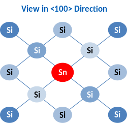
Silicon-tin or SiSn, is in general a term used for an alloy of the form Si(1-x)Snx. The molecular ratio of tin in silicon can vary based on the fabrication methods or doping conditions. In general, SiSn is known to be intrinsically semiconducting,[1] and even small amounts of Sn doping in silicon can also be used to create strain in the silicon lattice and alter the charge transport properties.[2]
Theoretical studies
Several theoretical works have shown SiSn to be semiconducting.[3][4] These mainly include DFT-based studies. The band structures obtained using these works show a change in band gap of silicon with the inclusion of tin into the silicon lattice. Thus, like SiGe, SiSn has a variable band gap that can be controlled using Sn concentration as a variable. In 2015, Hussain et al. experimentally verified the tuning of band gap associated with the diffusion of tin using homogeneous, abrupt p-n junction diodes.[5]
Production
SiSn can be obtained experimentally using several approaches. For small quantity of Sn in silicon, the Czochralski process is well known.[6][7] Diffusion of tin into silicon has also been tried extensively in the past.[8][9] Sn has the same valency and electronegativity as silicon and can be found in the diamond cubic crystal structure (α-Sn). Thus, silicon and tin meet three out of the four Hume-Rothery rules for solid state solubility. The one criterion that is not met is that of difference in atomic size. The tin atom is substantially larger than the silicon atom (31.8%). This reduces the solid state solubility of tin in silicon.[10]
Electrical performance
The first MOSFET (metal–oxide–semiconductor field-effect transistor) using SiSn as a channel material was shown in 2013.[11] This study proved that SiSn can be used as semiconductor for MOSFET fabrication, and that there may be certain applications where the use of SiSn instead of silicon may be more advantageous. In particular, the off current of SiSn transistors is much lower than that of silicon transistors.[12][13] Thus, logic circuits based on SiSn MOSFETs consume lower static power compared to silicon-based circuits. This is advantageous in battery operated devices (LSTP devices), where the standby power has to be reduced for longer battery life.
Thermal conductivity
Si-Sn alloys have the lowest conductivity (3 W/mK) of all the bulk alloys among Si-Ge, Ge-Sn, and Si-Ge-Sn; less than half that of Si-Ge which has been extensively studied, attributed to the larger difference in mass between the two constituents.[14] In addition, thin films offer an additional reduction in thermal conductivity, reaching around 1 W/mK in 20-nm-thick Si-Sn, Ge-Sn, and ternary Si-Ge-Sn films, which is near the conductivity of amorphous SiO2.[14] Group-IV alloys containing Sn have the potential for high-efficiency thermoelectric energy conversion.[14]
See also
References
- ↑ Jensen, Rasmus V S; Pedersen, Thomas G; Larsen, Arne N (31 August 2011). "Quasiparticle electronic and optical properties of the Si–Sn system". Journal of Physics: Condensed Matter 23 (34): 345501. doi:10.1088/0953-8984/23/34/345501. PMID 21841232. Bibcode: 2011JPCM...23H5501J.
- ↑ Simoen, E.; Claeys, C. (2000). "Tin Doping Effects in Silicon". Electrochem. Soc. Proc. 2000-17: 223.
- ↑ Amrane, Na.; Ait Abderrahmane, S.; Aourag, H. (August 1995). "Band structure calculation of GeSn and SiSn". Infrared Physics & Technology 36 (5): 843–848. doi:10.1016/1350-4495(95)00019-U. Bibcode: 1995InPhT..36..843A.
- ↑ Zaoui, A.; Ferhat, M.; Certier, M.; Khelifa, B.; Aourag, H. (June 1996). "Optical properties of SiSn and GeSn". Infrared Physics & Technology 37 (4): 483–488. doi:10.1016/1350-4495(95)00116-6. Bibcode: 1996InPhT..37..483Z.
- ↑ Hussain, Aftab M.; Wehbe, Nimer; Hussain, Muhammad M. (24 August 2015). "SiSn diodes: Theoretical analysis and experimental verification". Applied Physics Letters 107 (8): 082111. doi:10.1063/1.4929801. Bibcode: 2015ApPhL.107h2111H. https://repository.kaust.edu.sa/bitstream/10754/576462/1/1.4929801.pdf.
- ↑ Claeys, C.; Simoen, E.; Neimash, V. B.; Kraitchinskii, A.; Kras’ko, M.; Puzenko, O.; Blondeel, A.; Clauws, P. (2001). "Tin Doping of Silicon for Controlling Oxygen Precipitation and Radiation Hardness". Journal of the Electrochemical Society 148 (12): G738. doi:10.1149/1.1417558. Bibcode: 2001JElS..148G.738C.
- ↑ Chroneos, A.; Londos, C. A.; Sgourou, E. N. (2011). "Effect of tin doping on oxygen- and carbon-related defects in Czochralski silicon". Journal of Applied Physics 110 (9): 093507–093507–8. doi:10.1063/1.3658261. Bibcode: 2011JAP...110i3507C. http://oro.open.ac.uk/35250/1/Effect%20of%20tin%20doping.pdf.
- ↑ Kringhøj, Per; Larsen, Arne (September 1997). "Anomalous diffusion of tin in silicon". Physical Review B 56 (11): 6396–6399. doi:10.1103/PhysRevB.56.6396. Bibcode: 1997PhRvB..56.6396K.
- ↑ Yeh, T. H. (1968). "Diffusion of Tin into Silicon". Journal of Applied Physics 39 (9): 4266–4271. doi:10.1063/1.1656959. Bibcode: 1968JAP....39.4266Y.
- ↑ Akasaka, Youichi; Horie, Kazuo; Nakamura, Genshiro; Tsukamoto, Katsuhiro; Yukimoto, Yoshinori (October 1974). "Study of Tin Diffusion into Silicon by Backscattering Analysis". Japanese Journal of Applied Physics 13 (10): 1533–1540. doi:10.1143/JJAP.13.1533. Bibcode: 1974JaJAP..13.1533A.
- ↑ Hussain, Aftab M.; Fahad, Hossain M.; Singh, Nirpendra; Sevilla, Galo A. Torres; Schwingenschlögl, Udo; Hussain, Muhammad M. (2013). "Exploring SiSn as channel material for LSTP device applications". 71st Device Research Conference. pp. 93–94. doi:10.1109/DRC.2013.6633809. ISBN 978-1-4799-0814-1.
- ↑ Hussain, Aftab M.; Fahad, Hossain M.; Singh, Nirpendra; Sevilla, Galo A. Torres; Schwingenschlögl, Udo; Hussain, Muhammad M. (13 January 2014). "Tin - an unlikely ally for silicon field effect transistors?". Physica Status Solidi RRL 8 (4): 332–335. doi:10.1002/pssr.201308300. Bibcode: 2014PSSRR...8..332H.
- ↑ Hussain, Aftab M.; Fahad, Hossain M.; Singh, Nirpendra; Sevilla, Galo A. Torres; Schwingenschlögl, Udo; Hussain, Muhammad M. (2013). "Tin (Sn) for enhancing performance in silicon CMOS". 2013 IEEE 8th Nanotechnology Materials and Devices Conference (NMDC). pp. 13–15. doi:10.1109/NMDC.2013.6707470. ISBN 978-1-4799-3387-7.
- ↑ 14.0 14.1 14.2 Khatami, S. N. (2016). "Lattice Thermal Conductivity of the Binary and Ternary Group-IV Alloys Si-Sn, Ge-Sn, and Si-Ge-Sn". Physical Review Applied 6 (1): 014015. doi:10.1103/physrevapplied.6.014015. Bibcode: 2016PhRvP...6a4015K.
 |

