Engineering:Beyond CMOS
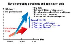
Beyond CMOS refers to the possible future digital logic technologies beyond the scaling limits of CMOS technology.[1][2][3][4] which limits device density and speeds due to heating effects.[5]
Beyond CMOS is the name of one of the 7 focus groups in ITRS 2.0 (2013) and in its successor, the International Roadmap for Devices and Systems.

CPUs using CMOS were released from 1986 (e.g. 12 MHz Intel 80386). As CMOS transistor dimensions were shrunk the clock speeds also increased. Since about 2004 CMOS CPU clock speeds have leveled off at about 3.5 GHz.

CMOS devices sizes continue to shrink – see Intel tick–tock and ITRS :
- 22 nanometer Ivy Bridge in 2012
- first 14 nanometer processors shipped in Q4 2014.
- In May 2015, Samsung Electronics showed a 300 mm wafer of 10 nanometer FinFET chips.[7]
It is not yet clear if CMOS transistors will still work below 3 nm.[4] See 3 nanometer.
Comparisons of technology
About 2010 the Nanoelectronic Research Initiative (NRI) studied various circuits in various technologies.[2]
Nikonov benchmarked (theoretically) many technologies in 2012,[2] and updated it in 2014.[8] The 2014 benchmarking included 11 electronic, 8 spintronic, 3 orbitronic, 2 ferroelectric, and 1 straintronics technology.[8]
The 2015 ITRS 2.0 report included a detailed chapter on Beyond CMOS,[9] covering RAM and logic gates.
Some areas of investigation
- Magneto-Electric Spin-Orbit logic[10]
- tunnel junction devices, eg Tunnel field-effect transistor[11]
- indium antimonide transistors
- carbon nanotube FET, eg CNT Tunnel field-effect transistor
- graphene nanoribbons
- molecular electronics
- spintronics — many variants
- future low-energy electronics technologies, ultra-low dissipation conduction paths, including
- photonics and optical computing
- superconducting computing
- rapid single-flux quantum (RSFQ)
Superconducting computing and RSFQ
Superconducting computing includes several beyond-CMOS technologies that use superconducting devices, namely Josephson junctions, for electronic signals processing and computing. One variant called rapid single-flux quantum (RSFQ) logic was considered promising by the NSA in a 2005 technology survey despite the drawback that available superconductors require cryogenic temperatures. More energy-efficient superconducting logic variants have been developed since 2005 and are being considered for use in large scale computing.[12][13]
See also
- International Technology Roadmap for Semiconductors
- International Roadmap for Devices and Systems
- Moore's law
- MOSFET scaling
- Nanostrain, a project to characterise piezoelectric materials for low power switches
- S-PULSE, the EU Shrink-Path of Ultra-Low Power Superconducting Electronics initiative
- Probabilistic complementary metal-oxide semiconductor (PCMOS)
References
- ↑ "Extending the road beyond CMOS. Hutchby 2002". https://web.stanford.edu/class/ee311/NOTES/Hutchby_ProcIEEE03.pdf.
- ↑ 2.0 2.1 2.2 Nikonov, Dmitri E.; Young, Ian A. (September 2012). "Overview of Beyond-CMOS Devices and A Uniform Methodology for Their Benchmarking". arXiv:1302.0244 [cond-mat.mes-hall].
- ↑ Bernstein (2011). Device and Architecture Outlook for Beyond CMOS Switches. https://www.fp7-nanotec.eu/content/device-and-architecture-outlook-beyond-cmos-switches-kerry-bernstein-wolfgang-porod-and-jeff. Retrieved 2015-02-22.
- ↑ 4.0 4.1 "Review of Advanced and Beyond CMOS FET Technologies for Radio Frequency Circuit Design. Carta 2011". http://www.mos-ak.org/dresden/publications/T4_Carta_MOS-AK_12.pdf.
- ↑ Frank, D.J. (March 2002). "Power-constrained CMOS scaling limits". IBM Journal of Research and Development 46 (2.3): 235–244. doi:10.1147/rd.462.0235.
- ↑ "Beyond CMOS". IEEE. 2018. https://irds.ieee.org/images/files/pdf/2017/2017IRDS_BC.pdf.
- ↑ "Samsung vows to start 10nm chip production in 2016". 23 May 2015. http://www.kitguru.net/components/anton-shilov/samsung-vows-to-start-10nm-chip-production-in-2016-shows-first-wafers/. Retrieved 16 July 2015.
- ↑ 8.0 8.1 Nikonov; Young (2015). "Benchmarking of Beyond-CMOS Exploratory – Devices for Logic Integrated Circuits". IEEE Journal on Exploratory Solid-State Computational Devices and Circuits 1: 3–11. doi:10.1109/JXCDC.2015.2418033. Bibcode: 2015IJESS...1....3N.
- ↑ Beyond CMOS. International Technology Roadmap for Semiconductors 2.0 (2015 ed.). https://www.dropbox.com/sh/3jfh5fq634b5yqu/AACxgvNR8zhcTYt2cp2nj0WOa/6_2015%20ITRS%202.0%20Beyond%20CMOS.pdf. Retrieved 2017-06-16.
- ↑ Manipatruni, Sasikanth; Nikonov, Dmitri E.; Lin, Chia-Ching; Gosavi, Tanay A.; Liu, Huichu; Prasad, Bhagwati; Huang, Yen-Lin; Bonturim, Everton et al. (2018-12-03). "Scalable energy-efficient magnetoelectric spin–orbit logic". Nature 565 (7737): 35–42. doi:10.1038/s41586-018-0770-2. ISSN 0028-0836. PMID 30510160. http://dx.doi.org/10.1038/s41586-018-0770-2.
- ↑ Seabaugh (September 2013). "The Tunneling Transistor". IEEE Spectrum (IEEE) 50 (10): 35–62. doi:10.1109/MSPEC.2013.6607013. https://spectrum.ieee.org/semiconductors/devices/the-tunneling-transistor. Retrieved 2023-04-16.
- ↑ Holmes, D.S.; Ripple, A.L.; Manheimer, M.A. (June 2013). "Energy-efficient superconducting computing—power budgets and requirements". IEEE Trans. Appl. Supercond. 23 (3): 1701610. doi:10.1109/TASC.2013.2244634. Bibcode: 2013ITAS...2301610H. https://ieeexplore.ieee.org/document/6449287. Retrieved 2023-04-16.
- ↑ Holmes, D.S.; Kadin, A.M.; Johnson, M.W. (December 2015). "Superconducting Computing in Large-Scale Hybrid Systems". Computer 48 (12): 34–42. doi:10.1109/MC.2015.375. https://ieeexplore.ieee.org/document/7368011. Retrieved 2023-04-16.
Further reading
- "New Door in the "Beyond CMOS" World". BISinfotech. 2019-09-03. https://www.bisinfotech.com/new-door-in-the-beyond-cmos-world/.
- Nikonov, Dmitri E.; Ian A. (2013-12). "Overview of Beyond-CMOS Devices and a Uniform Methodology for Their Benchmarking". Proceedings of the IEEE. 101 (12): 2498–2533. doi:10.1109/jproc.2013.2252317. ISSN 0018-9219.
- Seabaugh, A.C. and Zhang, Q., 2010. Low-voltage tunnel transistors for beyond CMOS logic. Proceedings of the IEEE, 98(12), pp.2095-2110.
- Bernstein, K., Cavin, R.K., Porod, W., Seabaugh, A. and Welser, J., 2010. Device and architecture outlook for beyond CMOS switches. Proceedings of the IEEE, 98(12), pp.2169-2184.
- Sasikanth Manipatruni, Nikonov, D.E. and Ian A. Young, 2018. Beyond CMOS computing with spin and polarization. Nature Physics, 14(4), pp.338-343.
- Banerjee, S.K., Register, L.F., Tutuc, E., Basu, D., Kim, S., Reddy, D. and MacDonald, A.H., 2010. Graphene for CMOS and beyond CMOS applications. Proceedings of the IEEE, 98(12), pp.2032-2046.
- Topaloglu, R.O. and Wong, H.S.P. eds., 2019. Beyond-CMOS technologies for next generation computer design. Berlin/Heidelberg, Germany: Springer.
- Sasikanth Manipatruni, Nikonov, D.E., Lin, C.C., Gosavi, T.A., Liu, H., Prasad, B., Huang, Y.L., Bonturim, E., Ramesh, R. and Young, I.A., 2019. Scalable energy-efficient magnetoelectric spin–orbit logic. Nature, 565(7737), pp.35-42.
External links
 |
