Engineering:Copper interconnects
Copper interconnects are used in integrated circuits to reduce propagation delays and power consumption. Since copper is a better conductor than aluminium, ICs using copper for their interconnects can have interconnects with narrower dimensions, and use less energy to pass electricity through them. Together, these effects lead to ICs with better performance. They were first introduced by IBM, with assistance from Motorola, in 1997.[1]
The transition from aluminium to copper required significant developments in fabrication techniques, including radically different methods for patterning the metal as well as the introduction of barrier metal layers to isolate the silicon from potentially damaging copper atoms.
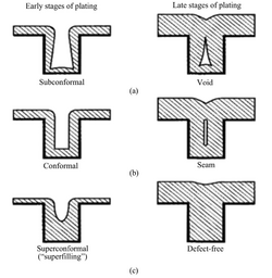
Although the methods of superconformal copper electrodeposition were known since late 1960, their application at the (sub)micron via scale (e.g. in microchips) started only in 1988–1995 (see figure). By the year 2002 it became a mature technology, and research and development efforts in this field started to decline.
Patterning
Although some form of volatile copper compound has been known to exist since 1947,[2] with more discovered as the century progressed,[3] none were in industrial use, so copper could not be patterned by the previous techniques of photoresist masking and plasma etching that had been used with great success with aluminium. The inability to plasma etch copper called for a drastic rethinking of the metal patterning process and the result of this rethinking was a process referred to as an additive patterning, also known as a "Damascene" or "dual-Damascene" process by analogy to a traditional technique of metal inlaying.[citation needed]
In this process, the underlying silicon oxide insulating layer is patterned with open trenches where the conductor should be. A thick coating of copper that significantly overfills the trenches is deposited on the insulator, and chemical-mechanical planarization (CMP) is used to remove the copper (known as overburden) that extends above the top of the insulating layer. Copper sunken within the trenches of the insulating layer is not removed and becomes the patterned conductor. Damascene processes generally form and fill a single feature with copper per Damascene stage. Dual-Damascene processes generally form and fill two features with copper at once, e.g., a trench overlying a via may both be filled with a single copper deposition using dual-Damascene.[citation needed]
With successive layers of insulator and copper, a multilayer interconnect structure is created. The number of layers depends on the IC's function, 10 or more metal layers are possible. Without the ability of CMP to remove the copper coating in a planar and uniform fashion, and without the ability of the CMP process to stop repeatably at the copper-insulator interface, this technology would not be realizable.[citation needed]
Barrier metal
A barrier metal layer must completely surround all copper interconnect, since diffusion of copper into surrounding materials would degrade their properties. For instance, silicon forms deep-level traps when doped with copper. As the name implies, a barrier metal must limit copper diffusivity sufficiently to chemically isolate the copper conductor from the silicon below, yet have high electrical conductivity in order to maintain a good electronic contact.
The thickness of the barrier film is also quite important; with too thin a layer, the copper contacts poison the very devices that they connect to; with too thick a layer, the stack of two barrier metal films and a copper conductor have a greater total resistance than aluminium interconnects, eliminating any benefit.
The improvement in conductivity in going from earlier aluminium to copper based conductors was modest, and not as good as to be expected by a simple comparison of bulk conductivities of aluminium and copper. The addition of barrier metals on all four sides of the copper conductor significantly reduces the cross-sectional area of the conductor that is composed of pure, low resistance, copper. Aluminium, while requiring a thin barrier metal to promote low ohmic resistance when making a contact directly to silicon or aluminium layers, did not require barrier metals on the sides of the metal lines to isolate aluminium from the surrounding silicon oxide insulators. Therefore scientists are looking for new ways to reduce the diffusion of copper into silicon substrates without using the buffer layer. One method is to use copper-germanium alloy as the interconnect material so that buffer layer (e.g. titanium nitride) is no longer needed. Epitaxial Cu3Ge layer has been fabricated with an average resistivity of 6 ± 1 μΩ cm and work function of ~4.47 ± 0.02 eV respectively,[4] qualifying it as a good alternative to copper.
Electromigration
Resistance to electromigration, the process by which a metal conductor changes shape under the influence of an electric current flowing through it and which eventually leads to the breaking of the conductor, is significantly better with copper than with aluminium. This improvement in electromigration resistance allows higher currents to flow through a given size copper conductor compared to aluminium. The combination of a modest increase in conductivity along with this improvement in electromigration resistance was to prove highly attractive. The overall benefits derived from these performance improvements were ultimately enough to drive full-scale investment in copper-based technologies and fabrication methods for high performance semiconductor devices, and copper-based processes continue to be the state of the art for the semiconductor industry today.
Superconformal electrodeposition of copper


Around 2005 the processor frequency reached 3 GHz due to continuous decrease in the on-chip transistor size in the previous years. At this point, the capacitive RC coupling of interconnects became the speed(frequency)-limiting factor.[5]
The process of reducing both R and C started in the late 1990's, when Al (aluminium) was replaced with Cu (copper) for lower R (resistance), and SiO2 was replaced with low-κ dielectrics for lower C (capacitance). Cu was selected as the replacement for Al, because it has the lowest electronic resistance among low-cost materials at room temperature, and because Cu shows a slower electromigration than Al. Noteworthy, in the case of Al interconnects was patterning process involves selective Al etching (i.e. subtractive manufacturing process) in uncoated areas, followed by deposition of a dielectric. Since no method of spatially-selective etching of copper was known, etching (patterning) of the dielectric was implemented instead. For the Cu deposition (i.e. an additive manufacturing process), the IBM team in the late 1990's selected electroplating. This started the 'copper revolution" in the semiconductor / microchip industry.
The copper plating starts with coating the walls of a via with a protective layer (Ta, TaN, SiN or SiC), that prevents Cu diffusion into silicon. Then, physical vapor deposition of a thin seed Cu layer on the via walls is performed.[6] This "seed layer" servers as the promoter for the next step of electrodeposition. Normally, due to slower mass-transport of Cu2+ ion, the electroplating is slower deep inside the vias. Under such conditions, via filling results in a formation of a void inside. In order to avoid such defects, bottom-up filling (or superconformal) filling is required, as shown in Fig. A.
Liquid solutions for superconformal copper electroplating typically comprise several additives in mM concentrations: chloride ion, a suppressor (such as polyethyleneglycol), an accelerator (e.g. bis(3-sulfopropyl)disulfide) and a leveling agent (e.g. Janus Green B).[7] Two main models for superconformal metal electroplating have been proposed:
1) curvature enhanced adsorbate concentration (CEAC) model suggests, that as the curvature of the copper layer on the bottom of the via increases, and the surface coverage of the adsorbed accelerator increases as well, facilitating kinetically limited Cu deposition in these areas. This model emphasizes the role of accelerator.
2) S-shaped negative differential resistance (S-NDR) model claims instead, that the main effect comes from the suppressor, which due to its high molecular weight/slow diffusion does not reach the bottom of the via and preferentially adsorbs at the top of the via, where it inhibits Cu plating.
There is experimental evidence to support either model. The reconciliatory opinion is that in the early stages of the bottom-up via filling the higher rate of Cu plating at the bottom is due to the lack of the PEG suppressor molecules there (their diffusion coefficienct is too low to provide a fast enough mass-transport). The accelerator, which is a smaller and faster diffusing molecule, reaches the bottom of the via, where it accelerates the rate of Cu plating without the suppressor. At the end of plating, the accelerator remains in a high concentration on the surface of the plated copper, causing the formation of a final bump.
See also
References
- ↑ "IBM100 - Copper Interconnects: The Evolution of Microprocessors". 7 March 2012. http://www-03.ibm.com/ibm/history/ibm100/us/en/icons/copperchip/.
- ↑ Kőrösy, F.; Misler, G (1947). "A Volatile Compound of Copper". Nature 160 (4053): 21. doi:10.1038/160021a0. PMID 20250932. Bibcode: 1947Natur.160...21K.
- ↑ Jeffries, Patrick M.; Wilson, Scott R.; Girolami, Gregory S. (1992). "Synthesis and characterization of volatile monomeric copper(II) fluoroalkoxides". Inorganic Chemistry 31 (22): 4503. doi:10.1021/ic00048a013.
- ↑ Wu, Fan; Cai, Wei; Gao, Jia; Loo, Yueh-Lin; Yao, Nan (2016-07-01). "Nanoscale electrical properties of epitaxial Cu3Ge film" (in en). Scientific Reports 6. doi:10.1038/srep28818. ISSN 2045-2322. PMID 27363582. Bibcode: 2016NatSR...628818W.
- ↑ Haumesser, 2016, 10.1016/b978-1-78548-092-8.50004-5
- ↑ Kim, 2022, 10.3390/electronics11182914
- ↑ Burkett, 2020, 10.1116/6.0000026
 |
