Engineering:Current differencing transconductance amplifier

Current differencing transconductance amplifier (CDTA) is a new active circuit element.
Properties
The CDTA is not free from parasitic input capacitances and it can operate in a wide frequency range due to current-mode operation. Some voltage and current mode applications using this element have already been reported in literature, particularly from the area of frequency filtering: general higher-order filters, biquad circuits, all-pass sections, gyrators, simulation of grounded and floating inductances and LCR ladder structures. Other studies propose CDTA-based high-frequency oscillators. Nonlinear CDTA applications are also expected, particularly precise rectifiers, current-mode Schmitt triggers for measuring purposes and signal generation, current-mode multipliers, etc.
Basic operation
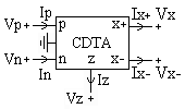
The CDTA element with its schematic symbol in Fig 1 has a pair of low-impedance current inputs and p, n and an auxiliary terminal z, whose outgoing current is the difference of input currents. Here, output terminal currents are equal in magnitude, but flow in opposite directions, and the product of transconductance () and the voltage at the z terminal gives their magnitudes. Therefore, this active element can be characterized with the following equations:
- ,
- ,
- ,
- .
where and is the external impedance connected to z terminal of the CDTA. CDTA can be thought as a combination of a current differencing unit followed by a dual-output operational transconductance amplifier, DO-OTA. Ideally, the OTA is assumed as an ideal voltage-controlled current source and can be described by , where Ix is output current, and denote non-inverting and inverting input voltage of the OTA, respectively. Note that gm is a function of the bias current. When this element is used in CDTA, one of its input terminals is grounded (e.g., ). With dual output availability, condition is assumed.
References
- Biolek, D.: CDTA – Building Block for Current- Mode Analog Signal Processing. In: Proceedings of the ECCTD’03, Kraków, Poland, Vol. III, (2003), 397-400
- Keskin A.Ü., Biolek, D., Hancioglu, E., Biolková, V: Current-mode KHN filter employing current differencing transconductance amplifiers, AEU - International Journal of Electronics and Communications, 60, (2006), 443-446
- Chen, H. Tsao, C. Chen,: Operational transresistance amplifier using CMOS technology. Electronic Letters., 28, 22 (1992), 2087–2088.
 |
