Engineering:ggNMOS
Grounded-gate NMOS, commonly known as ggNMOS, is an electrostatic discharge (ESD) protection device used within CMOS integrated circuits (ICs). Such devices are used to protect the inputs and outputs of an IC, which can be accessed off-chip (wire-bonded to the pins of a package or directly to a printed circuit board) and are therefore subject to ESD when touched. An ESD event can deliver a large amount of energy to the chip, potentially destroying input/output circuitry; a ggNMOS device or other ESD protective devices provide a safe path for current to flow, instead of through more sensitive circuitry. ESD protection by means of such devices or other techniques is important to product reliability: 35% of all IC failures in the field are associated with ESD damage.[1][2]

Structure
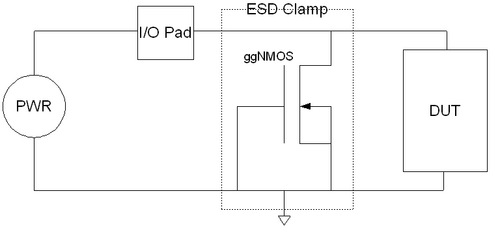
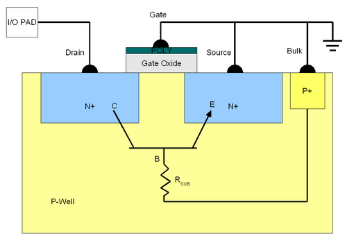
As the name implies, a ggNMOS device consists of a relatively wide NMOS device in which the gate, source, and body are tied together to ground. The drain of the ggNMOS is connected to the I/O pad under protection. A parasitic NPN bipolar junction transistor (BJT) is thus formed with the drain (n-type) acting as the collector, the base/source combination (n-type) as the emitter, and the substrate (p-type) as the base. As is explained below, a key element to the operation of the ggNMOS is the parasitic resistance present between the emitter and base terminals of the parasitic npn BJT. This resistance is a result of the finite conductivity of the p-type doped substrate.

Operation
When a positive ESD event appears upon the I/O pad (drain), the collector-base junction of the parasitic NPN BJT becomes reverse biased to the point of avalanche breakdown. At this point, the positive current flowing from the base to ground induces a voltage potential across the parasitic resistor, causing a positive voltage to appear across the base-emitter junction. The positive VBE forward biases this junction, triggering the parasitic NPN BJT.[3]
References
- ↑ Issaq, E.; Merri, R. (1993). "ESD design methodology". Electrical Overstress/Electrostatic Discharge Symposium. Lake Buena Vista, Florida. pp. 223-237.
- ↑ Green, T. (1988). "A review of EOS/ESD field failures in military equipment". Electrical Overstress/Electrostatic Discharge Symposium. Anaheim, California. pp. 7-14.
- ↑ Wang, Albert (2002). On-Chip ESD Protection for Integrated Circuits: An IC Design Perspective. Norwell, MA, USA: Kluwer Academic Publishing. ISBN 0792376471.
 |
