Engineering:Lattice and bridged-T equalizers
Lattice and bridged-T equalizers are circuits which are used to correct for the amplitude and/or phase errors of a network or transmission line. Usually, the aim is to achieve an overall system performance with a flat amplitude response and constant delay over a prescribed frequency range,[1]:128[2]:679 by the addition of an equalizer. In the past, designers have used a variety of techniques to realize their equalizer circuits. These include the method of complementary networks;[3]:438–534 the method of straight line asymptotes;[4] using a purpose built test-jig;[5] the use of standard circuit building blocks,;[3][6] or with the aid of computer programs.[7] In addition, trial and error methods have been found to be surprisingly effective,[8]:173[2][6] when performed by an experienced designer.
In video or audio channels, equalization results in waveforms that are transmitted with less degradation and have sharper transient edges with reduced overshoots (ringing)[9] than before. In other applications, such as CATV distribution systems[10] or frequency multiplexed telephone signals[11]:59 where multiple carrier signals are being passed, the aim is to equalize the transmission line so that those signals have much the same amplitude. The lattice and bridged-T circuits are favoured for passive equalizers because they can be configured as constant-resistance networks such as the Zobel network, as pointed out by Zobel[3] and later by Bode.[6]:249
The single word description “equalizer” is commonly used when the main purpose of the network is to correct the amplitude response of a system, even though some beneficial phase correction may also be achieved at same time.[6] When phase correction is the main concern, the more explicit term "phase equalizer" or "phase corrector" is used. (In this case, the circuit is usually an all-pass network which does not alter the amplitude response at all such as the lattice phase equalizer).
When equalizing a balanced transmission line, the lattice is the best circuit configuration to use, whereas for a single-ended circuit with an earth plane, the bridged-T network is more appropriate. Although equalizer circuits, of either form, can be designed to compensate for a wide range of amplitude and phase characteristics, they can become very complicated when the compensation task is difficult, as is shown later.
A variety of methods has been used to design equalizers and some of these are described below. Several of the procedures date back to the early part of the 20th century when equalizers were needed by the rapidly expanding telephone industry.[3] Later, with the advent of television, the equalisation of video links became very important too.[4]:713–738
Amplitude correction
The aim of an equalizer network is to correct for deficiencies in the amplitude response of a transmission line, lumped element network or amplifier chain. Equalisation is often necessary with transmission lines and lumped element delay lines which tend to have increasing loss with frequency. Without correction, waveform fidelity is lost, and rise and fall times of transients are degraded (i.e. less sharp).[12][13] Sometimes amplitude correction is required for more subtle reasons, for example, in the case of analogue colour television waveforms,[14] colour errors can occur in the displayed pictures when the transmission system’s response is not flat. It is usual to choose lattice and bridged-T equalizers which are constant-resistance networks. It was pointed out by Zobel[3] and later by Bode[6] that such networks can be cascaded with each other and with a transmission line or with a lumped element circuit, without introducing mismatch problems. The use of constant resistance configurations has been common practice in equalizer design, for many years, and almost all of the examples presented in this article have this property.
Whatever the design method, passive equalizers always introduce additional loss into the transmission path, and this has to be made good by an amplifier or repeater.
The method of complementary networks
In some of his early work, Zobel devised a lumped element circuit to simulate the behaviour of a given long transmission line of interest.[3] Such a device was useful in that it allowed investigatory work on a transmission system to be carried out in the convenience of the laboratory. Importantly, as was pointed out by Zobel, once such a network had been designed, it was always possible to find a realizable complementary network, which exhibited the inverse response.
An example
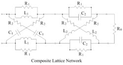
The procedure can be illustrated by a simple example presented by Zobel,[3]:470 which is shown below. Here, the left hand lattice has a simple low-pass characteristic and the right hand lattice has the complementary characteristic. For this circuit R1*R2 = L1/C1 = L2/C2 = R0^2 with R1 < 2.R0 .
C2 is given by [math]\displaystyle{ C_2 = \Big[ \Big(\frac{R_0}{R_1} \Big)^2-1 \Big].\frac{L_1}{R_0^2} }[/math]
For a normalized network R0 = 1Ω. Choose R1 = 0.5Ω and L1 = 1H then R2 = 2Ω, C1 = 1F, C2 = 3F, and L2 = 3H
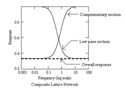
The responses of the individual sections and the overall response are shown in the plots for the composite network, given on the right.
This compensation process can be described mathematically, by means of the basic lattice equations given in lattice network, as follows. The transmission loss of a normalized (R0 = 1) constant resistance lattice with through arms Za and cross-diagonal arms of Zb is
[math]\displaystyle{ T(p) = \frac{1-z_a}{1+z_a} = \frac{z_b -1}{z_b+1} }[/math]
Now for the low-pass circuit, given above, za is a parallel combination of a 0.5Ω resistor in parallel with 1H inductor.
[math]\displaystyle{ z_a(lowpass)= \frac{0.5 \times p}{0.5 + p} = \frac{p}{1+2.p} }[/math]
and so
[math]\displaystyle{ T(lowpass) = \frac{1 - \frac{p}{(1+2.p}}{1 + \frac{p}{(1 + 2.p)}} = \frac{1 + p}{1 + 3.p} }[/math]
Next consider the high –pass section. Here za is a parallel combination of a 0.5Ω resistor in parallel with a 3F capacitor, so
[math]\displaystyle{ z_a(highpass)= \frac{0.5 \times 1/3.p}{0.5+1/3.p} = \frac{1}{2+3.p} }[/math]
and so
[math]\displaystyle{ T(highpass)=\frac{1-1/(2+3.p)}{1+1/(2+3.p)}= \frac{1+3.p}{3+3.p} = \frac{1+3.p}{3(1+p)} }[/math]
Finally, the overall response Ttot is
[math]\displaystyle{ T_{tot}(p)=T(lowpass) \times T(highpass) = \frac{1+p}{1+3.p} \times \frac{1+3.p}{3(1+p)} =\frac{1}{3} }[/math]
i.e. a flat response, with an overall gain of one third. This is shown in the figure above.
In this example, the overall characteristic is phaseless, i.e. full phase compensation has been achieved in addition to the amplitude correction. This is because exact correction has been achieved at all frequencies.[6]:249 Often correction is only successful over a limited range of frequencies, in which case the final result will have some residual phase.[15]:20
More generally, the response of a circuit or transmission line may be difficult to reproduce precisely by means of lumped element circuits, so the usual task is to find a realizable characteristic that is an acceptable match. Sometimes trial an error methods, applied in a systematic way can prove successful[2]:680[6]:274[1]:127
A general-purpose equalizer circuit
When the arms of a lattice network are purely reactive, constant resistance all-pass networks are possible, as shown in lattice delay network. If, however, resistors are included in the lattice arms, then different amplitude responses are possible while still retaining the constant resistance property.
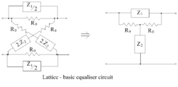
One, much-used equalizer circuit is shown here, together with the equivalent bridged-T circuit. The equivalence between the lattice and bridged-T can be shown with Bartlett's bisection theorem. The circuits have constant resistance characteristic when Z1.Z2 = R02.
The transfer function of this circuit is [math]\displaystyle{ T(p) = \frac{R_0}{R_0 + Z_1(p)} }[/math]
When normalized so that the source and terminating resistors and R0 are all unity and Z1.Z2 = 1, it becomes [math]\displaystyle{ T(p) = \frac{1}{1+Z_1(p)} }[/math]
and so Z1, as a function of T, is given by [math]\displaystyle{ Z_1(p) = \frac{1}{T(p)} -1 }[/math]
The simplicity of this equation (only one impedance has to be found) makes the circuit popular in equalizer designs.
The method of straight line asymptotes
The method uses an initial trial response, made up of a sequence of straight line asymptotes, to determine the pole/zero locations of a realizable network.[1]:131
The general principles of the method are as follows.
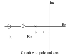
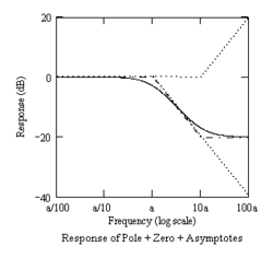
Consider the case of a simple RC low-pass circuit whose transfer function has a single pole on the real frequency axis at p = -a, as shown This response is -3 dB at ω = a and falls at 6 dB per octave at high frequencies. It is shown plotted, in decibels, versus frequency (on a log scale). Also shown, on the right, is the two-line asymptotic approximation, with break frequency also at ω = a. As can be seen, the true response and the straight line approximation are closely matched over most of the frequency range, only deviating near to ω = a.
If a zero is now added at, say, -10×a, then a new asymptote with a positive slope of 6 dB per octave is introduced, starting at ω = 10, as shown.
By extending the method, a complicated loss characteristic can be approximated by a sequence of straight line asymptotes provided the steepest slope of the loss characteristic does not exceed 6 dB per octave in the frequency range. The results are plotted on a dB scale against frequency on a log scale, as before.
In general, the transfer function is
[math]\displaystyle{ T(p)= \frac{(p+b)(p+d)(....}{(p+a)(p+c)(....}\quad where\ a\lt b\lt c\lt d\lt .... etc. }[/math]
Once an expression is deemed to meet the requirement with sufficient accuracy, the impedances Z1 and Z2 can be found from the relationships given earlier.
An example
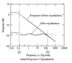
As an example, the transmission loss of a notional distribution network, with response shown by the full line in the figure on the left, is to be corrected (equalized). In this example correction is required over the frequency range from Ω1 = 0.09 r/s to Ω2 = 140 r/s. This can be approximated by a series of straight line segments as shown in the figure. Frequencies are chosen so that the various errors exhibited by the straight line approximation are all similar and as small as possible.
The straight line approximation shown in the figure has poles at ω = 0.333 r/s and 10 r/s, and zeros at ω = 1 r/s and 30 r/s.
The transfer function of a network with these poles and zeros is given by
[math]\displaystyle{ T(p) = \frac{(1+p)(1+0.03333p)}{(1+3p)(1+0.1p)} }[/math]
The actual response (magnitude) of T is easily calculated and is shown, on the plot on the right, as a function of frequency, together with the target response. A closer fit would require extra poles and zeros in T(p), at a closer spacing.
The low-pass network T(p), with this response will have an L-C network for Z1 and an R-C network for Z2, when realized using the simple circuits previously described. However, of more interest here is the complementary network, since this will correct for the falling transmission loss of this response.
The transfer function of the equalizer network will be [math]\displaystyle{ Te(p)= \frac{1}{T(p)} =\frac{1}{K}. \frac{(1+3p)(1+0.1p)}{(1+p)(1+0.03333p)} }[/math] where K = 9 so that the gain of the network never exceeds unity at any frequency.
The expression for Z1(p) can be derived from this equation using [math]\displaystyle{ Z_1(p)= \frac{1}{Te(p)} -1 }[/math]
So [math]\displaystyle{ Z_1(p) = \frac{8 + 6.2p}{(1+3p)(1+0.1p)} }[/math]
Z1 can be realized as an R-C ladder network (or as a parallel combination of two R-C impedances, each of which is a resistor and a capacitor in series).
A ladder network version of Z1 is shown on the left, together with that of Z2 (its dual network). Component values for Z1 (with R0 = 1) are: C1 = 0.04838F, C2 = 0.4747F, R1 = 2.2857Ω, R2 = 5.7152Ω and for Z2 they are L1 = 0.0438H, L2 = 0.4747H, R3 = 0.4375, R4 = 0.1750.
These circuits of Z1 and Z2 can be used directly into a bridged-T equalizer network, but for use in a lattice network, the capacitor values should be doubled and resistor values halved in the Z1 network, and all resistor and inductor values doubled in the Z2 (i.e. Za = Z1/2 and Zb = 2.Z2).
The overall response, when the equalizer is cascaded with the original characteristic, is shown on the right. As expected, there is ripple on the result, which is similar to the differences between the initial response and its approximation T(p).
Although the response, prior to equalization, considered in this example, has a characteristic which falls linearly when plotted against log(ω), it is possible to cope with non-linear characteristics in much the same way, provided the plot falls monotonically – i.e. the slope does not change sign, and the maximum slope is less than 6 dB/octave. In such cases, a series of straight line asymptotes can also be found to approximate a response and so lead to a realizable solution.
Equalizers of considerable complexity can be designed using the method of asymptotes, and they can achieve an overall, corrected, response with very low ripple (<<0.1 dB).[4]
Deriving compensation networks by means of an experimental test jig
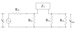
An experimental test jig may be used to find the component values to find circuit values for the equalizer.[5] The basic circuit arrangement is shown, on the left.
The transfer function of this simple circuit, ignoring flat loss, is [math]\displaystyle{ T(p)=\frac{R_0}{(R_0 + 2.Z_x)} }[/math]
Now, if 2.Zx = Z1, this becomes [math]\displaystyle{ T(p) = \frac{R_0}{(R_0 + Z_1)} }[/math]
So T(p) has the same form as the transfer function of the basic equalizer circuit given earlier with Zx identical to the “Za” lattice arms. So, although the test jig is not, in itself, a constant resistance network it does provide a convenient experimental method for determining the required component values for a lattice or bridged-T circuit which is a constant resistance network. Once the values of Zx are established, circuit values for Z1 and its dual, Z2, are found in a straightforward manner.
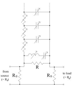
A suggested test jig,[5] using these concepts is shown, on the right.
(i) The basic R-C circuit that forms the bulk of Zx is in the form of a ladder network, rather than a parallel combination of series R-C pairs. The total spread in the capacitor values needed is much reduced for this configuration. Usually, a network of six or seven sections is sufficient. (ii) A shunt resistor R is placed across the input terminals of Zx, and this also reduces the spread of component values. Unfortunately, it also reduces the maximum correction possible by an individual equalizer section and may result in a cascade of two or more sections being necessary to achieve total equalisation. (iii) A series resonant L-C circuit is also present across the terminals of Zx. This combination is arranged to resonate above the top frequency of the system passband and its purpose is to reduce the equalizer flat loss. (It is a technique commonly used in equalizer circuits). (iv) Instead of finding component values to achieve a desirable frequency response, an alternative approach is to optimize the transient performance, by means of test waveforms (such as pulse and bar signals.,[16] for example). Optimizing transient performance in this way is particularly applicable to situations where waveform fidelity is important such as in television. When circuit values are obtained in this way, the description “waveform corrector” is preferred to “response equalizer”[5]
An example
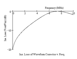
An example of a “waveform corrector” for a coaxial cable section for video frequencies[5] is shown. The shunt impedance Z2 is not shown in detail. It is the dual of Z1, so whereas Z1 contains a series resonant circuit and an R-C ladder network, Z2 contains a shunt resonant circuit and an R-L ladder network.
The plot of vout/vin (in dBs) versus frequency, for this circuit, using the component values proposed in the reference[5] is also shown, on the right.
Zobel’s curve fitting procedure
Zobel, in his early paper,[3] described a procedure in which a cascade of prototype constant resistance lattice networks formed the basis of his equalizers. His method was basically a curve fitting procedure and an Appendix in his paper provided a series of networks from which a complete equalizer could be built.[3]:512–534 He apportioned contributions to the overall desired equalizer response to the various members of a lattice (or bridged-T) cascade.
Each lattice circuit in the cascade was identified by its impedances Za and Zb (where Zb = R02/Za and by its “propagation function” and “attenuation constant” (in effect, the square of the magnitude).
These image parameters...[17] are all interrelated as Zobel demonstrated see (Image impedance).
Firstly, the lattice impedance Za can be expressed as the ratio of two polynomials in (jf)
[math]\displaystyle{ \frac{Z_1}{R} = \frac{a_0 + a_1(jf) + a_2(jf^2 + ....}{b_0 + b_1(jf) +b_2(jf)^2 + ....} }[/math]
In this expression, the impedance coefficients a0, b0, etc., one of which is unity and some may be zero, are algebraic combinations of the network elements. For any given type of network, the coefficients are fixed by the elements, and vice versa.
Secondly, the propagation constant Γ can be found from
[math]\displaystyle{ e^ \Gamma = \frac{g_0 +g_1(jf) +g_2(jf^2 + ....}{h_0 + h_1(jf) + h_2(jf)^2 + ....} }[/math]
in which g0, g1 ,h0, etc. are algebraic functions of a0, b0, etc. From this, the attenuation constant can be derived and expressed as a function of frequency. (It was the usual practice in the 1920s to display attenuation as a positive parameter, so the response of a low pass filter was displayed as a positively rising curve, with increasing frequency).
For the attenuation constant, the expression is of the form:
[math]\displaystyle{ F = (e^A)^2 = e^{2A} = 10^{ \frac{TU}{10}} = \frac{P_0 + P_2.f^2 +P_4.f^4 + ....}{Q_0 + Q_2.f^2 +Q_4.f^4 + ....} }[/math]
which is a ratio of two polynomials in f2, and in which the coefficients could be determined from the known data, or measurements.
Rearranging this, Zobel obtained the “attenuation linear equation”, which holds at all frequencies, thus:
[math]\displaystyle{ P_0 + f^2.P_2 + .... -FQ_0 - f^2Q_2 - .... = 0 }[/math]
By having attenuation data at sufficient data points (frequencies), a family of simultaneous equations can be solved to give the values of P0, Q0, P2, Q2, etc.
From these results, Zobel showed, in the Appendix of his paper how, for each prototype equalizer circuit, it was possible to derive the component values for that section.
An example
As an example, the procedure was used by Zobel to design an equalizer for a balanced line with a characteristic impedance of 600 Ω and 50 miles in length, for frequencies up to 4.5 kHz.[3]:480 In this early paper Zobel used the “napier” (the natural logarithm of a voltage ratio) and the “transmission unit” (a logarithm to the base 10 of a power ratio)[18] interchangeably within his calculations. The two units are related by 1 napier = 8.686 transmission units. In the mid 1920s these units were renamed[19] the “neper” and the “decibel" and these are the units used here.
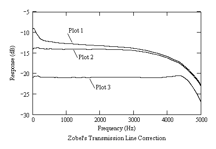
The original attenuation characteristic requiring correction is shown as “Plot 1” in the figure below.
Zobel proposed that a satisfactory equalized response would be obtained by a cascade of two lattices, of the types shown in the figure on the left. The left-hand lattice, in the figure, provided correction to the response at low frequencies and the right-hand one provided correction at high frequencies.
Considering first the left hand circuit, this has an attenuation linear equation
[math]\displaystyle{ P_0 + f^2.P_2 - F.Q_0 - f^2.Q_2 = f^4(F - 1) }[/math]
so there are four unknowns to find, P0, P2, Q0, Q2, and so data at four frequencies is required. From the measured data on the transmission line Zobel proposed the following attenuation values.
At f1 = 40 Hz, A1 = 0.536 neper; at f2 = 200 Hz, A2 = 0.291 neper; at f3 = 800 Hz, A3 = 0.176 neper; at f4 = 2000 Hz, A4 = 0.100 neper.
(These give a response which is the inverse of that of the original plot, as required for the equalizer, but with an arbitrary 0.1neper offset at the highest frequency.)
Solution of the four simultaneous equations derived from this data gave P0 = 102.007 ×10⁹, Q0 = 32.20010 ×10⁹, P2 = 5.06037 ×10⁶, Q2 = 3.43087 ×10⁶, from which Zobel’s design data gave the following component values: C1 = 1.2042 μF, R1 = 168.32 Ω, C2 = 4.0342 μF, R2 = 124.19 Ω R3 = 2138.72 Ω, L3 = 0.43351H, R44 = 2898.55 Ω, L4 = 1.4523H
In the case of the right-hand lattice chosen by Zobel, the attenuation constant has the same value at low and high frequencies, so P0 = F0 and it has a peak in the response near the resonant frequency of C6 and L6. The attenuation linear equation for this lattice is
[math]\displaystyle{ -P_2 +F.Q_2 -f^2(F_0 - F)Q_4 = (F_0 -F)/f^2 }[/math]
The expression for attenuation constant of the right hand lattice has P0 = F0, Q0 = 1 and P4 = F0.Q4, so data was needed to solve for P0, P2, Q2 and Q4. The data used was: at f0 = 0 Hz, A1 = 0.796 neper; at f1= 3000 Hz, A1 = 0.747 neper; at f2 = 4000 Hz, A2 = 0.530 neper; at f3 = 4500 Hz, A3 = 0.300 neper. The solution of the four simultaneous equations derived from this data gave F0 = P0 = 4.913; P2 = -46.207×10⁻⁸; Q2 = -90092×10−8; Q4 = 23.198×10⁻¹⁶ . Using this data, Zobel’s design equations for this lattice gave following component values: R5 = 226.95 Ω, R6 = 143.4 Ω, L6 = 0.04935H, C6 = .02476 μF R7 = 1586.25 Ω, R8 = 2510.46 Ω, L8 = 8.8992mH, C8 = 0.137 μF
The final results are shown in the figure below. Plot 1 of the figure shows the initial response of the cable run that was to be corrected. The compensation achieved by the left-hand (low frequency) lattice, alone, is shown in Plot 2. Finally, total compensation is shown in Plot 3, when the right-hand lattice is also included.
Bode’s method for equalisation
Bode devoted Chapter XII of his well known book[6] to the topic of equalizers. He pointed out that all transfer functions could be made up from a cascade of first and second order constant-resistance lattices which, of course, includes equalizer networks. In order to assist with the process of network design, Bode provided design details of four first and four second order networks to cover the various possible locations of the poles and zeros in the complex frequency plane. Unfortunately, some of the circuits he proposed (when pole and zero locations were complex), were derived using Brune’s synthesis method,[20] which sometimes produced lattice impedances containing mutually coupled coils. However, a later paper[21] provides alternative networks to avoid this problem.
An example
As an example of the method, consider the realization of the simple equalizer response given earlier. It can be realized by means of simple lattices in cascade. The response required is
[math]\displaystyle{ Te(p) = \frac{1}{T(p)} = \frac{1}{9}. \frac{(1 + 3p)(1 + 0.1p)}{(1 + p)(1 + 0.03333p} }[/math]
This can be rewritten thus
[math]\displaystyle{ Te(p) = \frac{(p + 0.3333p)}{(1 + p)}. \frac{(p + 10)}{(p + 30)} }[/math]
This can be apportioned to two first order lattices in cascade, using the Type IV circuits from Bode’s chart[6]:252 to give the circuit shown.
This can be easily converted to a cascade of standard constant resistance bridged-T sections of the form described earlier, as shown on the right. (Aa simpler circuit is also possible, which uses fewer resistors).
Development of an equalizer by circuit refinement
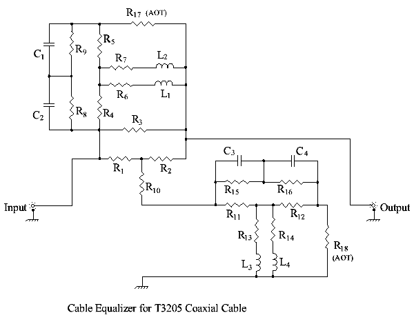
In addition to the methods described earlier, a final equalizer circuit may be obtained by first starting with an initial simple solution and then using a process of circuit refinement to increase the complexity of the circuit, and its response, until a satisfactory performance was obtained. An example of a commercially produced network, obtained in this way[22] is shown below. This equalizer was able to correct for the losses in various lengths of coaxial cable type BICC T3205 (a commercial high quality 75Ω video cable). The equalizer was a bridged-T circuit, rather than a lattice, as was appropriate for coaxial cable, Two versions of the circuit were produced, one for cable lengths of 0 to 100 feet and the second for cable lengths of 100 to 180 feet. Resistors R17 and R18 were “adjusted on test” (with R17×R18 = 752) to give optimum results for a given cable length.
Iterative procedures by computer programming
With the advent of modern computers, complex iterative routines can be run, which previously were prohibitively time consuming. Routines are possible which minimise the differences between an approximate trial solution and the target specification, either in a “least-squares” or “Chebyshev” sense.[23][15]:20 The programs use iterative procedures to successively solve linear programming problems, derived locally, as a way of dealing with non-linear problems.
An example
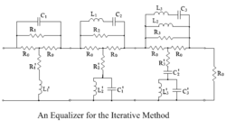
An example[23] illustrating the method, considered the insertion loss characteristic shown in “Attenuation Plot”, below.
A cascade of three lattice sections, as shown, was chosen to achieve the required equalizer response.
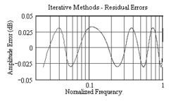
The component values, derived by the iteration procedure, gave a response which matched the characteristic in a Chebyshev sense, as required. The final result matched the target response at nine frequencies (there are nine degrees of freedom in the circuit R1 to R3, C1 to C3 and L1 to L3) with peak to peak errors of only ± 0.03 dB at intervening frequencies.
Variable equalizers
In the case of variable equalizers which are set by varying resistor values only, it is usual to use only Bridged-T networks because there are less components to match than in a lattice. Even then, to ensure a fully matched network, dual potentiometers are necessary.[24] Variable equalizers are also discussed by Rounds et al.[4] and Bode.[25] Bode was interested in variable equalizers adjusted by a single potentiometer, so his variable equalizers were not constant resistance networks.
Phase equalizers
Introduction
A phase equalizer is a circuit which is cascaded with a network in order to make the overall phase response more linear (or to make the group delay more constant). The combined circuit will transmit waveforms with improved fidelity, compared to the performance of the initial network alone.
Phase equalization is often necessary because many circuits are designed to achieve certain attenuation characteristics, with little regard paid to the phase characteristic that ensues. This is frequently the situation with filters for example, where, in the pursuit of a specific selectivity requirement, scant attention is paid to the phase response of the resulting network (as with Cauer’s filter design procedure[26]). Usually, the circuit produced is a minimum phase network, where sudden changes in the amplitude response always result in nonlinearities in the phase response, because of the precise relationship between amplitude and phase.[27] For example, a sharp-cut minimum phase low-pass filter, with a rapid transition from passband to stopband will always have a phase characteristic which deviates greatly from linear at frequencies in the vicinity of the cut-off frequency. The sharper the transition, the greater will be this deviation. (A plot of the group delay will also show a large increase in delay in the same frequency region).
Similarly, any amplitude ripple in the filter passband will also be accompanied by ripple of the phase characteristic. In many cases, both amplitude and phase ripples are undesirable and so there is little point in correcting for one type of ripple without also tackling the other[28]
If waveform fidelity is important, then a non-linear phase characteristics are undesirable. In television, for example, the pictorial defects attributable to phase distortion are excessive ringing of the luminance information and smeared and spurious colour edges at transitions in the colour information.[29]
In practice, phase correction procedures are most successful when applied to band limited systems, such as those containing a low pass or bandpass filter. This is because such filters inherently define a finite frequency band over which it is necessary to apply the correction.
As shown in lattice network, the lattice all-pass circuit is suitable as a phase correcting network because it is able to modify the phase characteristics of a filter network without introducing changes to its amplitude response. Also, the constant resistance property means that it does not create spurious reflections due to mismatch effects, when cascaded with other networks.
An example
As an example of the phase correction process, consider a conventional Butterworth low-pass filter of 9th order. The circuit, shown below, is the normalised filter, to be terminated with 1 ohm and with unity cut-off frequency).[30]:604
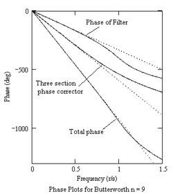
The amplitude and phase characteristics of this filter are given in the figures below. Also shown, in the left-hand plot, is the phase error curve for the filter (i.e. the deviation of the phase slope from linear). As can be seen in the right-hand plot, the phase slope of the low pass filter alone is linear at low frequencies but increases too rapidly at higher frequencies, ultimately resulting in a phase deviation, from linear, of 100 degrees near the top of the pass-band.
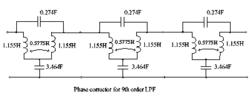
In order to correct for this phase deviation, the phase corrector needs a linear phase characteristic at low frequencies, but to be positive of the linear asymptote as the frequency increases. A cascade of three second order all-pass lattices will give the required phase characteristic for the filter, and their phase response is shown in the right hand plot. In this example, because the filter has an unbalanced form, it is necessary to use bridged-T equivalents in the phase corrector, rather than lattice circuits. The phase corrector is shown below. As the phase corrector is an all-pass and constant resistance circuit, it does not change the amplitude response of the filter.
The combined characteristic has a phase curve which is linear over the pass-band of the filter, but the resulting high phase slope means the combination has a significantly greater transmission delay than the filter alone.
In this example, the Butterworth low pass filter has nine poles, located at equi-angular intervals on a unity semi-circle in the left half of the complex frequency plane,[30]:495 and the poles and zeros of each of the three phase correctors are ±0.866 ±0.5j .
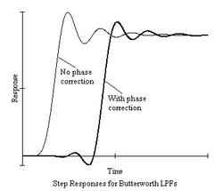
The transient behaviour of the filter, when subject to a step waveform is shown above. The first plot is for the filter, alone, without phase correction and the second plot shows the performance after correction. As expected the phase correction improves waveform symmetry, reduces the 10–90% rise-time, and roughly halves the peak amplitude of the overshoots, but it has increased the delay.
An overview of design methods for phase correctors
In practice, a variety of techniques have been used in the design of phase correctors. The simplest method uses trial and error procedures,[8]:173[2]:746[6]: 274 aided by a basic understanding of all-pass phase characteristics. The procedure can be surprisingly successful as, often, a cascade of a few phase correctors based on the maximally phase flat second order lattice will suffice [31]
A similar approach, based on the use of standard phase tables for equalizers with parabolic delay, allows the designer to determine the appropriate network to meet a given peak delay[32]
An improved procedure, noting that group delay characteristics of many networks could be considered as sums of parabolic and linear contributions, used charts and graphs in combination with three fitting techniques, namely the 3-point fit, the slope fit or the ‘averaged’ fit, to determine component values.[33]:162–187
Brain[34] described the phase correction of a cascade of 16 vacuum tubes interconnected by second order maximally flat inter-stage networks. The phase characteristic was derived from measurements of the amplitude response by using the relationship between amplitude and phase for minimum phase shift networks. Phase correction was accomplished by three identical second order phase correctors in the form of bridged-T networks.
Fredendhall[29] gave the pole-zero pattern and the circuit diagram for a four section delay equalizer which he proposed to the FCC should be used in transmitters to compensate for the characteristics of the ‘average’ receiver.
A more mathematical approach has been described which starts by choosing a basic cascade of phase correctors and then optimising their characteristics by a simple curve fitting procedure. A LPF for television use was designed by this method.[35]
More sophisticated still, an iterative convergence procedure has been run on a computer to optimise a cascade of phase correcting sections.[23] By having enough sections available to give the appropriate number of degrees of freedom, the desired phase characteristic can be achieved in a Chebyshev sense.
Another optimisation procedure[36] began by first noting that the delays of first and second order all-pass sections add linearly. So for a cascade of M first order and N second order networks, a best fit choice of M and N could be found to meet any given characteristic within acceptable bounds, by using a minimax approximation procedure. The process proceeded in two steps, the first was to find an approximation that coincided with the desired delay on a specified set of points. The second step consisted of perturbing those points in an attempt to find an equal ripple solution. By increasing the number of sections, chosen at the outset, the peak-peak ripple error can be made as small as required.
Szentirmai[37] has issued a computer aided design package called “S/FILSYN” which is capable of general purpose synthesis, including circuits for amplitude and phase equalization realised as lattice or bridged-T networks. He has also reviewed a number of other computer aided design packages[7]
See also
- Zobel network
- Lattice phase equalizer
- Lattice network
References
- ↑ 1.0 1.1 1.2 Stewart J.L., “Fundamentals of Signal Theory”, McGraw-Hill N.Y., 1960
- ↑ 2.0 2.1 2.2 2.3 Tuttle D.F., “Network Synthesis, Volume1”, Wiley, N.Y., 1958
- ↑ 3.0 3.1 3.2 3.3 3.4 3.5 3.6 3.7 3.8 3.9 Zobel O.J., “Distortion Correction in Electrical Circuits with Constant Resistance Recurrent Networks”, BSTJ Vol.7, No. 3, July 1928
- ↑ 4.0 4.1 4.2 4.3 Rounds P.W. and Lakin G.L., “Equalisation of Cables for Local Television Transmission”, BSTJ, Vol34, July 1955, (pp. 713–738)
- ↑ 5.0 5.1 5.2 5.3 5.4 5.5 Hale H.S. and MacDiarmid I.F., “Video waveform correctors for use with coaxial cable”, Proc. IEE, Vol 110, No. 8, August 1963, pp. 1319–1328
- ↑ 6.0 6.1 6.2 6.3 6.4 6.5 6.6 6.7 6.8 6.9 Bode H.W., “Network Analysis and Feedback Amplifier Design”, van Nostrand, 1945, reprinted Isha Books, India, 2013
- ↑ 7.0 7.1 Szentirmai G., "Computer-Aided Design Methods in Filter Design: S/FILSYN and Other Packages", Chapter 3 of "CRC Handbook of Electrical Filters", ed. Taylor J.T. and Huang Q., CRC Press, N.Y., 1996, pp. 19-41.
- ↑ 8.0 8.1 Stewart J.L., "Circuit Theory and Design", Wiley, N.Y., 1956
- ↑ Cherry C., “Pulses and transients in Communication Circuits”, Chapman & Hall, London, 1949, p.145
- ↑ Groffe D.E., “Bode’s Variable Equalizer”, NCTA Conference, April 1976, pp. 72–76
- ↑ Bray J., “Innovation and the Communications Revolution”, Institution of Electrical Engineers, London, 2002
- ↑ Terman F.E., “Voltage Amplifiers for Video Frequencies”, Electronic and Radio Engineering, Chapter 9, 4th Edition, N.Y. 1955, pp.288- 318
- ↑ Fink D.G., “IF Amplifiers and Detectors”, Television Engineering Handbook, Chapter 16.4, McGraw-Hill, N.Y., 1957, pp. 16.37–16.77
- ↑ Fink D.G., “Television Standards”, Television Engineering Handbook, Chapter 2, McGraw-Hill, N.Y., 1957, pp. 2.1–2.54
- ↑ 15.0 15.1 Rounds P.W., “Equalization of Video Cables”, Conv. Rec. IRE, Part 2, Circuit Theory, March 1954
- ↑ Hale H.S. and McDiarmid I.F., "Video waveform correctors for use with coaxial cable", Proc. IEE, Vol. 110, No.8, Aug. 1963, pp1319-1328
- ↑ Mathhaei G.L., Young L., Jones E.M.T., “Microwave Filters, Impedance-Matching Networks, and Coupling Structures”, Artch House, MA, 1980, pp. 49–81
- ↑ Martin W.H., “The Transmission Unit and Telephone Transmission System”, BSTJ, Vol. 3, July 1924, pp. 400–408
- ↑ Martin W.H., “The Name of the Transmission Unit”, BSTJ, Vol. 8, Jan 1929, pp.1–2
- ↑ Brune O., “Synthesis of a finite two-terminal network whose driving-point impedance is a prescribed function of frequency”, Jour. Math & Physics, Vol. 10, 1931, pp. 191–236
- ↑ Lee S.Y., “Extension of Bode’s Constant Resistance Lattice Synthesis of Transfer Impedance Function”, BSTJ, Vol. 48, 1969, pp. 637–657
- ↑ EMI, “Cable Equalizer”, Drawing number 9A/B/C910086/A & B
- ↑ 23.0 23.1 23.2 Ishizaki Y. and Watanabe H., “An Iterative Chebyshev Approximation Method for Network Design”, IEEE Trans on Circuit Theory, Vol. CT-15, No.4, Dec 1968
- ↑ Groffe D.E., “Bode’s Variable Equalizers”, NCTA Conference, April 1976, pp. 72–76
- ↑ Bode H.W. “Variable Equalizers”, BSTJ, Vol. 17, April 1938, pp. 229–244
- ↑ Guillemin E.A., “Communication Networks, Volume II”, Wiley, N.Y., 1935, pp. 394–412
- ↑ Bode H.W., “Relations Between Amplitude and Phase in Feedback Amplifier Design”, BSTJ, Vol. 19, 1940, pp. 421–454
- ↑ Wheeler H.A., "The Interpretation of Amplitude and Phase Distortion in Terms of Paired Echoes", Proc. IRE, Vol. 27, Issue 6, June 1939, pp. 359–384
- ↑ 29.0 29.1 Fredendall G.L., “Delay Equalization in Color Television”, Proc. IRE, Jan. 1954, (pp. 258–262))
- ↑ 30.0 30.1 Weinberg L, “Network Analysis and Synthesis”, McGraw-Hill, N.Y., 1962
- ↑ Brain A.E. “The Compensation for Phase Errors in Wide-Band Video Amplifiers”, Proc. IEE, Vol. 97, Iss. 48, Part III Radio & Comms.).
- ↑ Cunningham V.R., “Pick a delay equalizer”, Electronic Design, May 1966, pp. 62–66
- ↑ Skwirzynski J.K. and Dunlop E.J., “Group Delay Equalisation of Bandpass Filters at Intermediate Frequencies”, Marconi Review, 4th Quarter, 1964
- ↑ Brain A.E., The Compensation for Phase Errors in Wide-Band Video Amplifiers", Proc. IEE, Part III, Radio & Comms., Vol.97, Iss. 48, pp. 243–252
- ↑ Head J.W. and Howorth D., “Design and Group-delay Correction of a Low-pass Filter for use in Video Circuits”, Electronic Engineering, August 1966 (pp. 520–524)
- ↑ Crane R.L., “All-Pass Network Synthesis”, IEEE Trans on Circuit Theory, Dec 1969 (p. 474).
- ↑ Szentirmai G., “FILSYN v. 1.70 for Windows”, 2013. Find at http://www.Alkeng.com/sfilsyn.html
 |
