Engineering:MOS Technology Agnus

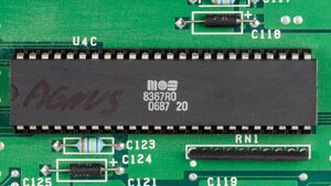
The MOS Technology "Agnus", usually called Agnus, is an integrated circuit in the custom chipset of the Amiga computer. The Agnus, Denise and Paula chips collectively formed the OCS and ECS chipsets.
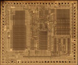
The Agnus is the Address Generator Chip. Its main function, in chip area, is the RAM Address Generator and Register Address Encoder which handles all DMA addresses. The 8361 Agnus is made up of approximately 21000 transistors and contains DMA Channel Controllers. According to Jay Miner, original Agnus was fabricated in 5 μm manufacturing process like all OCS chipset. The Blitter and Copper are also contained here.
Agnus features:
- The Blitter, a bitmap manipulator. The Blitter is capable of copying blocks of display data, or any arbitrary data in the on-board memory, at high speed with various raster operations as well as drawing pixel perfect lines and filling outlined polygons, while freeing the CPU for concurrent tasks.
- "Copper", a display synchronized co-processor
- 25 Direct Memory Access (DMA) channels, allowing graphics, sound and I/O to be used with minimal CPU intervention
- DRAM refresh controller
- Memory controller (memory that can be accessed by the processor and the chipset)
- Generates the system clock from the 28 MHz oscillator
- Video timing
Agnus was replaced by Alice in the Amiga 4000 and Amiga 1200 when the AGA chipset was introduced in 1992.
Chips by capability

- OCS Agnus which can address up to 512 kB of Chip RAM (PLCC versions add 512 kB of pseudo-fast RAM)
- 8361 (DIP) - Amiga 1000 (NTSC); Amiga 2000 model A (NTSC)
- 8367 (DIP) - Amiga 1000 (PAL); Amiga 2000 model A (PAL)
- 8370 (PLCC) - Amiga 500 to Rev 5.x (NTSC); Amiga 2000 model B to Rev 4.5 (NTSC)
- 8371 (PLCC) - Amiga 500 to Rev 5.x (PAL); Amiga 2000 model B to Rev 4.5 (PAL)
- ECS Agnus which can address up to 1 MB of Chip RAM
- 8372 - no data*
- 8372A - Amiga 500 from Rev 6 (NTSC/PAL); Amiga 2000 model B from Rev 6.0 to Rev 6.3 (NTSC/PAL); Commodore CDTV
- 8375 (318069-16 only) (PAL) - Amiga 500 from Rev 6 (PAL); Amiga 2000 model B from Rev 6.4 (PAL)
- 8375 (318069-17 only) (NTSC) - Amiga 500 from Rev 6 (NTSC); Amiga 2000 model B from Rev 6.4 (NTSC)
- ECS Agnus which can address up to 2 MB of Chip RAM
- 8372AB - Amiga 3000 from Rev 6.1 to Rev 8.9 (NTSC/PAL)
- 8372B - Amiga 3000 Rev 9 (NTSC/PAL)
- 8375 (PAL) - Amiga 500 Plus; Amiga 600 (PAL)
- 8375 (NTSC) - Amiga 600 (NTSC)
* Somewhere 8372A Agnus mentioned as simply "8372".
Chips by package
- 48-lead DIP Agnus (aka thin Agnus): 8361; 8367
- 84-contact PLCC Fat Agnus (named Fat Lady on most Amiga 2000 motherboards) 8370; 8371; 8372; 8372A; 8372AB; 8372B; 8375
Notes
Fat Agnus 1MB and Fat Agnus 2MB usually known as Super Agnus; Super Fat Agnus; Fatter Agnus; Big Agnus; Big Fat Agnus, but these aren't official names.
DMA Channels
| Priority | Name | Count | Cycles/Rasterline | Chip | Notes |
|---|---|---|---|---|---|
| MPU | 1 | varying | CPU | ||
| A | Blitter | 4 | varying | Agnus (internal) | yields 1/4 cycles to CPU when BLTPRI not active |
| B | Bitplane | 6 | 80 | Denise | impairs sprite channels on severe overscan |
| C | Copper | 1 | varying | Agnus (internal) | |
| D | Audio | 4 | 4 | Paula | |
| E | Sprites | 8 | 16 | Denise | |
| F | Disk | 1 | 3 | Paula | |
| G | Memory Refresh | 1 | 4 | - | |
| Reference: Amiga 500 plus Service Manual | |||||
Pinout
PLCC Versions
When replacing or upgrading chips, pinouts need to be taken care of. Types are just mentioned for reference; four-digit types and pinouts/usage are not consistent.[1]
| Pin | OCS/ECS | ECS | AGA (Alice) | Description | |
|---|---|---|---|---|---|
| A500/2000 | A3000 | A500+/600 | A4000/1200 | ||
| 8370/1 | 8372 | 8375 | 8374 | ||
| 1 | RD13 | DRD13 | DRD13 | DRD13 | Data Bus 16 bit, bit 13 |
| 2 | RD12 | DRD12 | DRD12 | DRD12 | . . . |
| 3 | RD11 | DRD11 | DRD11 | DRD11 | |
| 4 | RD10 | DRD10 | DRD10 | DRD10 | |
| 5 | RD9 | DRD9 | DRD9 | DRD9 | |
| 6 | RD8 | DRD8 | DRD8 | DRD8 | |
| 7 | RD7 | DRD7 | DRD7 | DRD7 | |
| 8 | RD6 | DRD6 | DRD6 | DRD6 | |
| 9 | RD5 | DRD5 | DRD5 | DRD5 | |
| 10 | RD4 | DRD4 | DRD4 | DRD4 | |
| 11 | RD3 | DRD3 | DRD3 | DRD3 | |
| 12 | RD2 | DRD2 | DRD2 | DRD2 | |
| 13 | RD1 | DRD1 | DRD1 | DRD1 | |
| 14 | RD0 | DRD0 | DRD0 | DRD0 | Data Bus 16 bit, bit 0 |
| 15 | Vcc | Vcc | Vcc | Vcc1 | +5V ±5% |
| 16 | RST* | _RESET | _RESET | /RESET | Global RESETn, low active |
| 17 | INT3 | _INTR | _INTR | /INTR | |
| 18 | DMAL | DMAL | DMAL | DMAL | |
| 19 | BLS* | _BLISS | _BLISS | /BLS | |
| 20 | DBR* | _BLIT | _BLIT | /DBR | |
| 21 | RRW | _WE | _WE | /WE | |
| 22 | PRW | R/W | R/W | R/W | |
| 23 | RGEN* | _REGEN | _REGEN | _REGEN | |
| 24 | AS* | _AS | _AS | NC2 | |
| 25 | RAMEN* | _RAMEN | _RAMEN | /RAMEN | |
| 26 | RGA8 | RGA8 | RGA8 | RGA8 | |
| 27 | RGA7 | RGA7 | RGA7 | RGA7 | |
| 28 | RGA6 | RGA6 | RGA6 | RGA6 | |
| 29 | RGA5 | RGA5 | RGA5 | RGA5 | |
| 30 | RGA4 | RGA4 | RGA4 | RGA4 | |
| 31 | RGA3 | RGA3 | RGA3 | RGA3 | |
| 32 | RGA2 | RGA2 | RGA2 | RGA2 | |
| 33 | RGA1 | RGA1 | RGA1 | RGA1 | |
| 34 | 28 MHz | 28 MHz | 28 MHz | SCLK | |
| 35 | XCLK | A20 | A20 | A20 | |
| 36 | XCLKEN* | _XCLKEN | _CDAC | 14 MHz | |
| 37 | CDAC* | _CDAC | 7 MHz | /CDAC | |
| 38 | 7 MHz | 7 MHz | CCKQ | 7 MHz | |
| 39 | CCKQ | CCKQ | CCK | CCKQ | |
| 40 | CCK | CCK | 14M | CCK | |
| 41 | TEST | TEST | GND | /NTSC | |
| 42 | Vss | Vss1 | DRA0 | GND2 | |
| 43 | MA0 | DRA0 | DRA1 | DRA0 | Memory address bus 9 bit, bit 0 (except 8375 which is bit 1) |
| 44 | MA1 | DRA1 | DRA2 | DRA1 | . . . |
| 45 | MA2 | DRA2 | DRA3 | DRA2 | |
| 46 | MA3 | DRA3 | DRA4 | DRA3 | |
| 47 | MA4 | DRA4 | DRA5 | DRA4 | |
| 48 | MA5 | DRA5 | DRA6 | DRA5 | |
| 49 | MA6 | DRA6 | DRA7 | DRA6 | |
| 50 | MA7 | DRA7 | DRA8 | DRA7 | |
| 51 | MA8 | DRA8 | _LDS | DRA8 | Memory address bus 9 bit, bit 8 (except 8375 which is bit _LDS) |
| 52 | LDS* | _LDS | _UDS | Vcc2 | |
| 53 | UDS* | _UDS | _CASL | NC1 | |
| 54 | CASL* | _CASL | _CASU | /CAS | |
| 55 | CASU* | _CASU | DRA9 | Vbb | |
| 56 | RAS1* | DRA9 | _RAS1 | DRA9 | |
| 57 | RAS0* | _RAS | _RAS0 | /RAS | |
| 58 | Vss | Vss2 | GND | GND3 | |
| 59 | A19 | A19 | A19 | A19 | |
| 60 | A1 | A1 | A1 | A1 | |
| 61 | A2 | A2 | A2 | A2 | |
| 62 | A3 | A3 | A3 | A3 | |
| 63 | A4 | A4 | A4 | A4 | |
| 64 | A5 | A5 | A5 | A5 | |
| 65 | A6 | A6 | A6 | A6 | |
| 66 | A7 | A7 | A7 | A7 | |
| 67 | A8 | A8 | A8 | A8 | |
| 68 | A9 | A9 | A9 | A9 | |
| 69 | A10 | A10 | A10 | A10 | |
| 70 | A11 | A11 | A11 | A11 | |
| 71 | A12 | A12 | A12 | A12 | |
| 72 | A13 | A13 | A13 | A13 | |
| 73 | A14 | A14 | A14 | A14 | |
| 74 | A15 | A15 | A15 | A15 | |
| 75 | A16 | A16 | A16 | A16 | |
| 76 | A17 | A17 | A17 | A17 | |
| 77 | A18 | A18 | A18 | A18 | |
| 78 | LP* | _LPEN | _LPEN | /LPEN | |
| 79 | VSY* | _VSYNC | _VSYNC | /VSYNC | |
| 80 | CSY* | _CSYNC | _CSYNC | /CSYNC | |
| 81 | HSY* | _HSYNC | _HSYNC | /HSYNC | |
| 82 | Vss | Vss3 | GND | GND1 | Ground, common on whole board |
| 83 | RD15 | DRD15 | DRD15 | DRD15 | Data Bus 16 bit, bit 15 |
| 84 | RD14 | DRD14 | DRD14 | DRD14 | Data Bus 16 bit, bit 14 |
References: A500 Service Training, A3000 Service Manual, A500+ Service Manual, A1200 schematics
See also
References
- Sources
- AMIGA 1000 ASSEMBLY LEVEL REPAIR (Commodore-Amiga, Inc.) 1985 PN 314038-01 Dave's Amiga Schematics and Manuals
- Commodore Amiga A500/A2000 Technical Reference Manual (Commodore-Amiga, Inc.) 1987 Dave's Amiga Schematics and Manuals
- A500 SYSTEM SCHEMATICS COMPONENT PART LIST (Rev 6A/7) Dave's Amiga Schematics and Manuals
- A3000 SYSTEM SCHEMATICS (Commodore Business Machines, Inc.) March, 1990 PN-314677-01 www.1000bit.net
- CDTV SERVICE MANUAL (Commodore International Spare GmbH) May, 1991 PN-400403-01 www.ianstedman.co.uk (ZIP-file)
- A500 PLUS SERVICE MANUAL (Commodore International Spare GmbH) October, 1991 PN-400420-01 www.1000bit.net
- A600 SYSTEM SCHEMATICS (Commodore International Spare GmbH) April, 1992 PN-400422-02 www.1000bit.net
- OBLIGEMENT: les chipsets de l'Amiga
- Big Book of Amiga Hardware
- alexh on English Amiga Board (Agnus 8372B info)
- National Amiga Inc. mirrored on l8r.net
- Marketed Commodore Amiga models
- AMIGA Auckland Inc.
- Amiga University
- Commodore Computer Online Museum
- Notes
- ↑ George Robbins (14 October 1992). "Difference of 8372A vs 8375". Newsgroup: comp.sys.amiga.hardware. Usenet: 35861@cbmvax.commodore.com. Retrieved 1 October 2018.
