Engineering:Oxide thin-film transistor

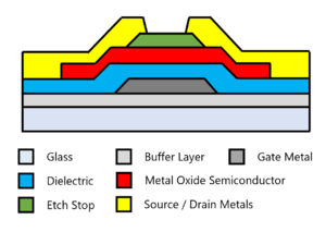
An oxide thin-film transistor (oxide TFT) or metal oxide thin film transistor is a type of thin film transistor where the semiconductor is a metal oxide compound. An oxide TFT is distinct from a metal oxide field effect transistor (MOSFET) where the word "oxide" refers to the insulating gate dielectric (normally silicon dioxide). In an oxide TFT, the word oxide refers to the semiconductor. Oxide TFTs have applications as amplifiers to deliver current to emitters in display backplanes.
History
The first transistor employing a metal oxide as the semiconductor was reported in 1964 by Klasens and Koelmans at Philips Research Laboratories.[1] However, oxide TFTs were seldom considered again for several decades after this. It wasn't until the early 2000's that Hideo Hosono, who was studying transparent conducting oxides,[2] discovered that oxysulfides[3] and indium gallium zinc oxide[4][5] could be used as semiconductors in TFTs. Soon after, John Wager at Oregon State University reported oxide TFTs employing the binary oxide zinc oxide as the semiconductor.[6]
Properties
Oxides have several properties which make them desirable over hydrogenated amorphous silicon (a-Si:H), which was the incumbent TFT technology in the early 2000's.[7] Firstly, the electron mobility is roughly 100 times higher in oxide TFTs.[8] Because the source-drain current in transistors is linearly proportional to electron mobility,[9] so too are the amplification properties. The result of this is that smaller transistors can be used to provide the same current. In a display this means that a higher resolution and switching speed is possible.
a-Si:H additionally suffers from issues with environmental stability, such as the Staebler-Wronski Effect.[10] As oxides are already oxidized, they are generally more environmentally stable, however they do experience a phenomenon called Negative Bias Illumination Stress (NBIS) where the threshold voltage changes under constant illumination.[11]
Most n-type (electron transporting) oxide TFTs employ semiconductors that have a wide bandgap; generally greater than 3 eV. For this reason they are attractive for use in fully transparent electronics. Their wide bandgap also means they have a low off-current, and hence a high on/off ratio; a desirable property for well-defined on- and off-states.
One significant drawback with oxide TFTs is that there are very few p-type (hole transporting) metal oxide semiconductors.[12] While not a significant problem when providing amplification to emitters, this does mean oxide semiconductors are less suitable for complementary logic, and hence information processing.
Growth
Metal oxide semiconductors are typically deposited using sputtering, a vacuum-based growth technique resulting in an amorphous or polycrystalline layer. Oxides can also be deposited from solution, such as via spin-coating or spray coating.[13]
Commercial use
Several companies have adopted oxide TFTs as a platform for display drivers. Notably Sharp in 2012,[14] and Apple in 2013.[15]
References
- ↑ Klasens, H.A.; Koelmans, H. (1964-09-01). "A tin oxide field-effect transistor" (in en). Solid-State Electronics 7 (9): 701–702. doi:10.1016/0038-1101(64)90057-7. ISSN 0038-1101. Bibcode: 1964SSEle...7..701K. https://www.sciencedirect.com/science/article/abs/pii/0038110164900577.
- ↑ Hosono, Hideo; Yasukawa, Masahiro; Kawazoe, Hiroshi (1996-08-01). "Novel oxide amorphous semiconductors: transparent conducting amorphous oxides" (in en). Journal of Non-Crystalline Solids 203: 334–344. doi:10.1016/0022-3093(96)00367-5. ISSN 0022-3093. Bibcode: 1996JNCS..203..334H. https://www.sciencedirect.com/science/article/abs/pii/0022309396003675.
- ↑ Ueda, K.; Inoue, S.; Hirose, S.; Kawazoe, H.; Hosono, H. (2000-10-16). "Transparent p-type semiconductor: LaCuOS layered oxysulfide". Applied Physics Letters 77 (17): 2701–2703. doi:10.1063/1.1319507. ISSN 0003-6951. Bibcode: 2000ApPhL..77.2701U. https://aip.scitation.org/doi/10.1063/1.1319507.
- ↑ Nomura, Kenji; Ohta, Hiromichi; Ueda, Kazushige; Kamiya, Toshio; Hirano, Masahiro; Hosono, Hideo (2003-05-23). "Thin-Film Transistor Fabricated in Single-Crystalline Transparent Oxide Semiconductor" (in en). Science 300 (5623): 1269–1272. doi:10.1126/science.1083212. ISSN 0036-8075. PMID 12764192. Bibcode: 2003Sci...300.1269N. https://www.science.org/doi/10.1126/science.1083212.
- ↑ Hosono, Hideo (July 2018). "How we made the IGZO transistor" (in en). Nature Electronics 1 (7): 428. doi:10.1038/s41928-018-0106-0. ISSN 2520-1131.
- ↑ Hoffman, R. L.; Norris, B. J.; Wager, J. F. (2003-01-28). "ZnO-based transparent thin-film transistors". Applied Physics Letters 82 (5): 733–735. doi:10.1063/1.1542677. ISSN 0003-6951. Bibcode: 2003ApPhL..82..733H. https://aip.scitation.org/doi/abs/10.1063/1.1542677.
- ↑ Brotherton, S. D. (2013) (in en). Introduction to Thin Film Transistors: Physics and Technology of TFTs. Springer International Publishing. ISBN 978-3-319-00001-5. https://www.springer.com/gp/book/9783319000015.
- ↑ Kamiya, Toshio; Nomura, Kenji; Hosono, Hideo (2010-02-01). "Present status of amorphous In–Ga–Zn–O thin-film transistors". Science and Technology of Advanced Materials 11 (4). doi:10.1088/1468-6996/11/4/044305. ISSN 1468-6996. PMID 27877346.
- ↑ Sze, S.M.; Ng, Kwok K. (2006-04-10) (in en). Physics of Semiconductor Devices. doi:10.1002/0470068329. ISBN 978-0-470-06832-8. https://onlinelibrary.wiley.com/doi/book/10.1002/0470068329.
- ↑ Staebler, D. L.; Wronski, C. R. (1977-08-15). "Reversible conductivity changes in discharge‐produced amorphous Si". Applied Physics Letters 31 (4): 292–294. doi:10.1063/1.89674. ISSN 0003-6951. Bibcode: 1977ApPhL..31..292S. https://aip.scitation.org/doi/10.1063/1.89674.
- ↑ Nomura, Kenji; Kamiya, Toshio; Hosono, Hideo (2010). "Interface and bulk effects for bias—light-illumination instability in amorphous-In—Ga—Zn—O thin-film transistors" (in en). Journal of the Society for Information Display 18 (10): 789–795. doi:10.1889/JSID18.10.789. ISSN 1938-3657. https://sid.onlinelibrary.wiley.com/doi/abs/10.1889/JSID18.10.789.
- ↑ Wang, Zhenwei; Nayak, Pradipta K.; Caraveo-Frescas, Jesus A.; Alshareef, Husam N. (2016). "Recent Developments in p-Type Oxide Semiconductor Materials and Devices" (in en). Advanced Materials 28 (20): 3831–3892. doi:10.1002/adma.201503080. ISSN 1521-4095. PMID 26879813. https://onlinelibrary.wiley.com/doi/abs/10.1002/adma.201503080.
- ↑ Thomas, Stuart R.; Pattanasattayavong, Pichaya; Anthopoulos, Thomas D. (2013-07-22). "Solution-processable metal oxide semiconductors for thin-film transistor applications" (in en). Chemical Society Reviews 42 (16): 6910–6923. doi:10.1039/C3CS35402D. ISSN 1460-4744. PMID 23770615. https://pubs.rsc.org/en/content/articlelanding/2013/cs/c3cs35402d.
- ↑ "Sharp begins to produce Oxide TFT (IGZO) based LCDs | OLED-Info". https://www.oled-info.com/sharp-begins-produce-oxide-tft-igzo-based-lcds.
- ↑ "IGZO display tech finally makes it to mass market: iPad Air now, high-res desktop display soon - ExtremeTech". https://www.extremetech.com/computing/170970-igzo-display-tech-finally-makes-it-to-mass-market-ipad-air-now-high-res-laptops-and-desktops-next.
 |
