Engineering:Photoconductance decay
Photoconductance decay or Photoconductivity decay (PCD or PC), is a non-destructive analytical technique used to measure the lifetime of minority charge carriers in a semiconductor, especially in silicon wafers.[1] The technique studies the transient photoconductivity of a semiconductor sample during or after it is illuminated by a light pulse. Electron–hole pairs are first generated by the light pulse, and the photoconductivity of the sample declines as the carriers recombine.
PCD is an important characterisation step in determining the quality and expected performance of wafers before they are used to fabricate devices such as integrated circuits or solar cells. It is one of the most common methods of determining carrier lifetimes.[2]
PCD uses a fast light source (e.g. a xenon flash lamp) to excite the test sample, causing free carriers to be generated. Excess carriers in the material cause it to become more conductive, and thus the number of excess carriers () can be measured over time by measuring the material conductivity. Conductivity can be measured through non-contact methods, such as through microwave reflectance, or inductive or capacitive coupling.[3] A higher effective lifetime of minority charge carriers indicate that they can remain mobile in the wafer for a long time period before undergoing recombination.
History
Characterisation of minority carrier lifetimes through measurement of photoconductance decay was a technique used by Bell Laboratories as early as 1954 on silicon and germanium wafers during investigation of carrier trapping.[4] A detailed method for measuring PCD was published soon after by MIT Lincoln Laboratory in 1955.[5] A standard method for PCD was described in ATSM standards in 1971 for measurement of minority carrier lifetimes.[1] A new method for Quasi-steady-state photoconductance measurements was described in 1996 by Ronald Sinton.[3]
Theory

The difference in dark and excited photoconductivity of the wafer is typically measured through monitoring of the voltage across the induction coil beneath the wafer. This yields a conductance that is spatially averaged over the coil area. Conductance can be related to the excess carrier generation by;[3][6]
where and are excess electrons and holes, and are the electron and hole mobilities respectively, is the wafer thickness and is the elementary charge. It can be assumed that as electrons and holes are always generated in pairs.
When the conductance is obtained, the average can be calculated from the semiconductor parameters;
Depending on the expected lifetime of the material relative to the illumination decay characteristics of the flash lamp, there are several modes that can be used for PCD measurements.
The generalised equation for effective lifetimes as a function of the excess carrier density is given by;[7]
|
|
() |
where is the generation rate as measured by a photodetector. The generalised case can be used regardless of the wafer lifetime or flash lamp.
Alternatively, the limiting cases of this function can be exploited in either quasi-transient or quasi-steady-state photoconductance (QSS-PC) measurements.
Transient PCD is used when the of the material is expected to exceed the flash duration, and the PCD measurement is taken after the light source has completely decayed. In this case, is assumed to be 0, and Equation (1) can be reduced to;
For materials in which the effective lifetime is expected to be shorter than the flash lamp decay time, carriers are assumed to be continuously generated (i.e. at steady state), and therefore . Therefore, Equation (1) can be reduced to;
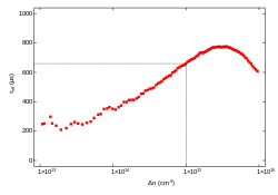
The case to be used is determined experimentally. The effective lifetimes is then calculated through curve fitting of the function and evaluated at a specified minority carrier density set-point, typically (see figure).
Applications

Recombination through the Shockley–Read–Hall (SRH) method is associated with the density of defects (such as contaminant atoms, dangling bonds, crystal grain boundaries, mechanical damage, etc.) in the semiconductor which "trap" charge carriers, leading to reduced lifetimes. Thus PCD can be used to infer the purity or passivation quality of the wafer. In solar cell production, this is particularly useful when estimating the performance of a precursor early in its manufacturing stage. Charge carriers that recombine cannot be used for photocurrent extraction, therefore for higher solar cell efficiency it is desirable to have a higher effective lifetime.
The minority carrier lifetime is also related to the open-circuit voltage of a solar cell, and therefore can be used to infer an implicit current–voltage characteristic of the finished solar cell.[8]
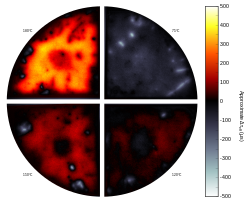
Lifetimes measurements from PCD can be used to quantitatively calibrate spatially-resolved lifetimes measurements from Photoluminescence (PL) imaging.[9] Minority carrier lifetimes are higher when there are fewer trap defects, and in the absence of SRH recombination, radiative recombination becomes more dominant. After excitation, radiatively recombining carriers emit nearly monochromatic light at the band gap energy of the semiconductor sample. For silicon, the energy is 1.12eV (in infrared) which can be captured by a CCD camera. Areas of the image with higher PL counts are inferred to have proportionately higher lifetimes.
See also
References
- ↑ 1.0 1.1 Bielle-Daspet, D.M.; Johan, A.M.; Espioussas, F. (1980). "Carrier lifetime measurements from transient electrical photoresponses". Revue de Physique Appliquée 15 (2): 219–227. doi:10.1051/rphysap:01980001502021900. ISSN 0035-1687. http://www.edpsciences.org/10.1051/rphysap:01980001502021900.
- ↑ "Carrier Lifetimes" (in en), Semiconductor Material and Device Characterization (Hoboken, NJ, USA: John Wiley & Sons, Inc.): pp. 389–464, 2005-04-07, doi:10.1002/0471749095.ch7, ISBN 978-0-471-73906-7, https://onlinelibrary.wiley.com/doi/10.1002/0471749095.ch7, retrieved 2023-03-19
- ↑ 3.0 3.1 3.2 Sinton, R.A.; Cuevas, A.; Stuckings, M. (May 1996). "Quasi-steady-state photoconductance, a new method for solar cell material and device characterization". Conference Record of the Twenty Fifth IEEE Photovoltaic Specialists Conference - 1996. pp. 457–460. doi:10.1109/PVSC.1996.564042. ISBN 0-7803-3166-4.
- ↑ Haynes, J. R.; Hornbeck, J. A. (1953-04-01). "Temporary Traps in Silicon and Germanium" (in en). Physical Review 90 (1): 152–153. doi:10.1103/PhysRev.90.152.2. ISSN 0031-899X. Bibcode: 1953PhRv...90..152H. https://link.aps.org/doi/10.1103/PhysRev.90.152.2.
- ↑ Stevenson, Donald T.; Keyes, Robert J. (February 1955). "Measurement of Carrier Lifetimes in Germanium and Silicon" (in en). Journal of Applied Physics 26 (2): 190–195. doi:10.1063/1.1721958. ISSN 0021-8979. Bibcode: 1955JAP....26..190S. http://aip.scitation.org/doi/10.1063/1.1721958.
- ↑ Drummond, P. J.; Bhatia, D.; Kshirsagar, A.; Ramani, S.; Ruzyllo, J. (2011-09-01). "Studies of photoconductance decay method for characterization of near-surface electrical properties of semiconductors" (in en). Thin Solid Films 519 (22): 7621–7626. doi:10.1016/j.tsf.2011.04.212. ISSN 0040-6090. Bibcode: 2011TSF...519.7621D. https://www.sciencedirect.com/science/article/pii/S0040609011010595.
- ↑ Nagel, Henning; Berge, Christopher; Aberle, Armin G. (December 1999). "Generalized analysis of quasi-steady-state and quasi-transient measurements of carrier lifetimes in semiconductors" (in en). Journal of Applied Physics 86 (11): 6218–6221. doi:10.1063/1.371633. ISSN 0021-8979. Bibcode: 1999JAP....86.6218N. http://aip.scitation.org/doi/10.1063/1.371633.
- ↑ Sinton, Ronald A.; Cuevas, Andres (21 October 1996). "Contactless determination of current–voltage characteristics and minority-carrier lifetimes in semiconductors from quasi-steady-state photoconductance data" (in en). Applied Physics Letters 69 (17): 2510–2512. doi:10.1063/1.117723. ISSN 0003-6951. Bibcode: 1996ApPhL..69.2510S. http://aip.scitation.org/doi/10.1063/1.117723.
- ↑ Herlufsen, Sandra; Schmidt, Jan; Hinken, David; Bothe, Karsten; Brendel, Rolf (December 2008). "Photoconductance-calibrated photoluminescence lifetime imaging of crystalline silicon: Photoconductance-calibrated PL lifetime imaging of crystalline silicon" (in en). Physica Status Solidi RRL 2 (6): 245–247. doi:10.1002/pssr.200802192. https://onlinelibrary.wiley.com/doi/10.1002/pssr.200802192.
 |
