Engineering:Plasma etching
Plasma etching is a form of plasma processing used to fabricate integrated circuits. It involves a high-speed stream of glow discharge (plasma) of an appropriate gas mixture being shot (in pulses) at a sample. The plasma source, known as etch species, can be either charged (ions) or neutral (atoms and radicals). During the process, the plasma generates volatile etch products at room temperature from the chemical reactions between the elements of the material etched and the reactive species generated by the plasma. Eventually the atoms of the shot element embed themselves at or just below the surface of the target, thus modifying the physical properties of the target.[1]
Mechanisms
Plasma generation
A plasma is a high energetic condition in which a lot of processes can occur. These processes happen because of electrons and atoms. To form the plasma electrons have to be accelerated to gain energy. Highly energetic electrons transfer the energy to atoms by collisions. Three different processes can occur because of this collisions:[2][3]
Different species are present in the plasma such as electrons, ions, radicals, and neutral particles. Those species are interacting with each other constantly. Two processes occur during plasma etching:[4]
- generation of chemical species
- interaction with the surrounding surfaces
Without a plasma, all those processes would occur at a higher temperature. There are different ways to change the plasma chemistry and get different kinds of plasma etching or plasma depositions. One way to form a plasma is by using RF excitation by a power source of 13.56 MHz, a frequency allocated for this application in the ISM bands.
The mode of operation of the plasma system will change if the operating pressure changes. Also, it is different for different structures of the reaction chamber. In the simple case, the electrode structure is symmetrical, and the sample is placed upon the grounded electrode.
Influences on the process
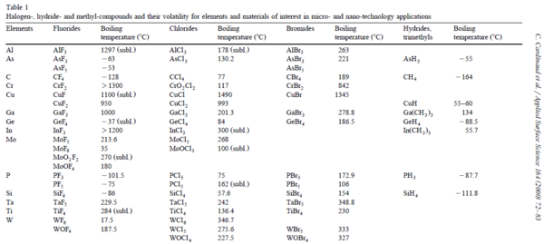
The key to develop successful complex etching processes is to find the appropriate gas etch chemistry that will form volatile products with the material to be etched as shown in Table 1.[3] For some difficult materials (such as magnetic materials), the volatility can only be obtained when the wafer temperature is increased. The main factors that influence the plasma process:[2][3][5]
- Electron source
- Pressure
- Gas species
- Vacuum

Surface interaction
The reaction of the products depend on the likelihood of dissimilar atoms, photons, or radicals reacting to form chemical compounds. The temperature of the surface also affects the reaction of products. Adsorption happens when a substance is able to gather and reach the surface in a condensed layer, ranging in thickness (usually a thin, oxidized layer.) Volatile products desorb in the plasma phase and help the plasma etching process as the material interacts with the sample's walls. If the products are not volatile, a thin film will form at the surface of the material. Different principles that affect a sample's ability for plasma etching:[3][6]
- Volatility
- Adsorption
- Chemical Affinity
- Ion-bombarding
- Sputtering
Plasma etching can change the surface contact angles, such as hydrophilic to hydrophobic, or vice versa. Argon plasma etching has reported to enhance contact angle from 52 deg to 68 deg,[7] and, Oxygen plasma etching to reduce contact angle from 52 deg to 19 deg for CFRP composites for bone plate applications. Plasma etching has been reported to reduce the surface roughness from hundreds of nanometers to as much lower as 3 nm for metals.[8]
Types
Pressure influences the plasma etching process. For plasma etching to happen, the chamber has to be under low pressure, less than 100 Pa. In order to generate low-pressure plasma, the gas has to be ionized. The ionization happens by a glow charge. Those excitations happen by an external source, which can deliver up to 30 kW and frequencies from 50 Hz (dc) over 5–10 Hz (pulsed dc) to radio and microwave frequency (MHz-GHz).[2][9]
Microwave plasma etching
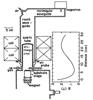
Microwave etching happens with an excitation sources in the microwave frequency, so between MHz and GHz. One example of plasma etching is shown here.[10]

Hydrogen plasma etching
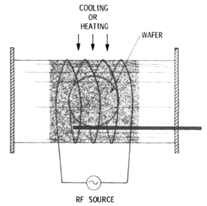
One form to use gas as plasma etching is hydrogen plasma etching. Therefore, an experimental apparatus like this can be used:[5]

Plasma etcher
A plasma etcher, or etching tool, is a tool used in the production of semiconductor devices. A plasma etcher produces a plasma from a process gas, typically oxygen or a fluorine-bearing gas, using a high frequency electric field, typically 13.56 MHz. A silicon wafer is placed in the plasma etcher, and the air is evacuated from the process chamber using a system of vacuum pumps. Then a process gas is introduced at low pressure, and is excited into a plasma through dielectric breakdown.
Plasma confinement
Industrial plasma etchers often feature plasma confinement to enable repeatable etch rates and precise spatial distributions in RF plasmas.[11] One method of confining plasmas is by using the properties of the Debye sheath, a near-surface layer in plasmas similar to the double layer in other fluids. For example, if the Debye sheath length on a slotted quartz part is at least half the width of the slot, the sheath will close off the slot and confine the plasma, while still permitting uncharged particles to pass through the slot.
Applications
Plasma etching is currently used to process semiconducting materials for their use in the fabrication of electronics. Small features can be etched into the surface of the semiconducting material in order to be more efficient or enhance certain properties when used in electronic devices.[3] For example, plasma etching can be used to create deep trenches on the surface of silicon for uses in microelectromechanical systems. This application suggests that plasma etching also has the potential to play a major role in the production of microelectronics.[3] Similarly, research is currently being done on how the process can be adjusted to the nanometer scale.[3]
Hydrogen plasma etching, in particular, has other interesting applications. When used in the process of etching semiconductors, hydrogen plasma etching has been shown to be effective in removing portions of native oxides found on the surface.[5] Hydrogen plasma etching also tends to leave a clean and chemically balanced surface, which is ideal for a number of applications.[5]
Oxygen plasma etching can be used for anisotropic deep-etching of diamond nanostructures by application of high bias in inductively coupled plasma/reactive ion etching (ICP/RIE) reactor.[12] On the other hand, the use of oxygen 0V bias plasmas can be used for isotropic surface termination of C-H terminated diamond surface.[13]
Integrated circuits
Plasma can be used to grow a silicon dioxide film on a silicon wafer (using an oxygen plasma), or can be used to remove silicon dioxide by using a fluorine bearing gas. When used in conjunction with photolithography, silicon dioxide can be selectively applied or removed to trace paths for circuits.
For the formation of integrated circuits it is necessary to structure various layers. This can be done with a plasma etcher. Before etching, a photoresist is deposited on the surface, illuminated through a mask, and developed. The dry etch is then performed so that structured etching is achieved. After the process, the remaining photoresist has to be removed. This is also done in a special plasma etcher, called an asher.[14]
Dry etching allows a reproducible, uniform etching of all materials used in silicon and III-V semiconductor technology. By using inductively coupled plasma/reactive ion etching (ICP/RIE), even hardest materials like e.g. diamond can be nanostructured.[15][16]
Plasma etchers are also used for de-layering integrated circuits in failure analysis.
Printed circuit boards
Plasma is used to etch printed circuit boards, including de-smear vias.[17]
See also
References
- ↑ "Plasma Etch - Plasma Etching". oxinst.com. http://www.oxinst.com/products/etching-deposition-growth/processes-techniques/plasma-etch/Pages/plasma-etch.aspx.
- ↑ 2.0 2.1 2.2 Mattox, Donald M. (1998). Handbook of Physical Vapor Deposition (PVD) Processing. Westwood, New Jersey: Noyes Publication.
- ↑ 3.0 3.1 3.2 3.3 3.4 3.5 3.6 Cardinaud, Christophe; Peignon, Marie-Claude; Tessier, Pierre-Yves (2000-09-01). "Plasma etching: principles, mechanisms, application to micro- and nano-technologies". Applied Surface Science. Surface Science in Micro & Nanotechnology 164 (1–4): 72–83. doi:10.1016/S0169-4332(00)00328-7. Bibcode: 2000ApSS..164...72C.
- ↑ Coburn, J. W.; Winters, Harold F. (1979-03-01). "Plasma etching—A discussion of mechanisms". Journal of Vacuum Science & Technology 16 (2): 391–403. doi:10.1116/1.569958. ISSN 0022-5355. Bibcode: 1979JVST...16..391C.
- ↑ 5.0 5.1 5.2 5.3 Chang, R. P. H.; Chang, C. C.; Darac, S. (1982-01-01). "Hydrogen plasma etching of semiconductors and their oxides". Journal of Vacuum Science & Technology 20 (1): 45–50. doi:10.1116/1.571307. ISSN 0022-5355. Bibcode: 1982JVST...20...45C.
- ↑ Coburn, J. W.; Winters, Harold F. (1979-05-01). "Ion- and electron-assisted gas-surface chemistry—An important effect in plasma etching". Journal of Applied Physics 50 (5): 3189–3196. doi:10.1063/1.326355. ISSN 0021-8979. Bibcode: 1979JAP....50.3189C.
- ↑ Zia, A. W.; Wang, Y. -Q.; Lee, S. (2015). "Effect of Physical and Chemical Plasma Etching on Surface Wettability of Carbon Fiber-Reinforced Polymer Composites for Bone Plate Applications". Advances in Polymer Technology 34: n/a. doi:10.1002/adv.21480.
- ↑ Wasy, A.; Balakrishnan, G.; Lee, S. H.; Kim, J. K.; Kim, D. G.; Kim, T. G.; Song, J. I. (2014). "Argon plasma treatment on metal substrates and effects on diamond-like carbon (DLC) coating properties". Crystal Research and Technology 49 (1): 55–62. doi:10.1002/crat.201300171. Bibcode: 2014CryRT..49...55W.
- ↑ Bunshah, Rointan F. (2001). Deposition Technologies for Films and Coatings. New York: Noyes Publication.
- ↑ Keizo Suzuki; Sadayuki Okudaira; Norriyuki Sakudo; Ichiro Kanomata (Nov 11, 1977). "Microwave Plasma Etching". Japanese Journal of Applied Physics 16 (11): 1979–1984. doi:10.1143/jjap.16.1979. Bibcode: 1977JaJAP..16.1979S.
- ↑ "Ignition conditions for peripheral plasma in a grounded chamber connected to a dual frequency capacitive discharge". http://www.eecs.berkeley.edu/~lieber/confinedphys20Apr05.pdf.
- ↑ Radtke, Mariusz; Nelz, Richard; Slablab, Abdallah; Neu, Elke (2019). "Reliable Nanofabrication of Single-Crystal Diamond Photonic Nanostructures for Nanoscale Sensing". Micromachines 10 (11): 718. doi:10.3390/mi10110718. PMID 31653033. Bibcode: 2019arXiv190912011R.
- ↑ Radtke, Mariusz; Render, Lara; Nelz, Richard; Neu, Elke (2019). "Plasma treatments and photonic nanostructures for shallow nitrogen vacancy centers in diamond". Optical Materials Express 9 (12): 4716. doi:10.1364/OME.9.004716. Bibcode: 2019OMExp...9.4716R.
- ↑ "Hochtechnologie - Weltweit | PVA TePla AG". http://www.pvatepla.com/en/products/plasma-systems/microwellen-plasma/photoresist-ashing/overview.
- ↑ Radtke, Mariusz; Nelz, Richard; Slablab, Abdallah; Neu, Elke (2019-10-24). "Reliable Nanofabrication of Single-Crystal Diamond Photonic Nanostructures for Nanoscale Sensing". Micromachines (MDPI AG) 10 (11): 718. doi:10.3390/mi10110718. ISSN 2072-666X. PMID 31653033.
- ↑ Radtke, Mariusz; Render, Lara; Nelz, Richard; Neu, Elke (2019-11-21). "Plasma treatments and photonic nanostructures for shallow nitrogen vacancy centers in diamond". Optical Materials Express (The Optical Society) 9 (12): 4716. doi:10.1364/ome.9.004716. ISSN 2159-3930. Bibcode: 2019OMExp...9.4716R.
- ↑ Lee, Eung Suok; Park, Hae II; Baik, Hong Koo; Lee, Se-Jong; Song, Kie Moon; Hwang, Myung Keun; Huh, Chang Su (2003). "Air mesh plasma for PCB de-smear process". Surface and Coatings Technology 171 (1–3): 328–332. doi:10.1016/S0257-8972(03)00295-0. https://www.sciencedirect.com/science/article/abs/pii/S0257897203002950.
External links
 |
