Engineering:TO-5


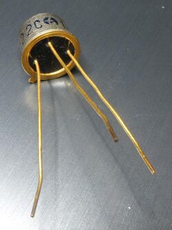
In electronics, TO-5 is a designation for a standardized metal semiconductor package used for transistors and some integrated circuits. The TO element stands for "transistor outline" and refers to a series of technical drawings produced by JEDEC.[1] The first commercial silicon transistors, the 2N696 and 2N697 from Fairchild Semiconductor, came in a TO-5 package.[2]
Construction and orientation
The tab is located 45° from pin 1, which is typically the emitter. The typical TO-5 package has a base diameter of 8.9 mm (0.35 in), a cap diameter of 8.1 mm (0.32 in), a cap height of 6.3 mm (0.25 in).[1] The pins are isolated from the package by individual glass-metal seals, or by a single resin potting. Sometimes one pin is connected directly to the metal case.
Variants
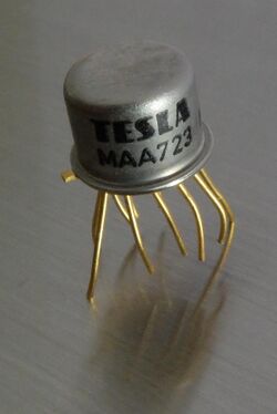
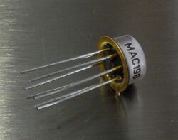
Several variants of the original TO-5 package have the same cap dimensions but differ in the number and length of the leads (wires). Somewhat incorrectly, TO-5 and TO-39 are often used in manufacturer's literature as synonyms for any package with the cap dimensions of TO-5, regardless of the number of leads, or even for any package with the diameter of TO-5, regardless of the cap height and the number of leads.[3] Compared to TO-5, for the other variants (except TO-33 and TO-42) the minimum length of the leads was shortened from 38.1 mm (1.50 in) to 12.7 mm (0.50 in) which is sufficient for through-hole technology and leads to a cost reduction, whereas the longer leads were needed for point-to-point construction. Lead lengths of 25.4 mm (1.00 in) and 19.05 mm (0.750 in) are quite common but were not standardized separately by JEDEC. There are variants with between 2 and 12 leads. The leads are arranged in a circle with a diameter of 5.08 mm (0.200 in) (except TO-96, TO-97, TO-100, TO-101). Before the introduction of dual in-line packages in 1965, integrated circuits were packaged mostly in metal can packages such as the TO-5 variants with more than 3 leads.[4]
TO-39 / TO-9 / TO-16 / TO-42
The TO-39, TO-9, and TO-16 packages have 3 leads and differ in the shortened leads mentioned above from TO-5.[5] Additionally, the TO-9 and TO-16 packages do not have a tab.[6] The TO-42 package is almost identical to the TO-5 package (including the long leads) but has four stand-offs at the bottom of the base that keep the base about 0.5 mm above the circuit board.[7] Possibly the TO-16 and TO-42 designations were not actually used.[2]
TO-12 / TO-33

The TO-12 and TO-33 packages have 4 leads.[8] TO-33 has 38.1 mm (1.50 in) leads[9] like TO-5 while TO-12 has 12.7 mm (0.50 in) leads. For transistors, the fourth wire is typically connected to the metal case as a means of electromagnetic shielding for radio frequency applications.
TO-75
The TO-75 package has 6 leads (at most one of those may be omitted).[10] The minimum angle between two adjacent leads is 60°.
TO-76 / TO-77

The TO-76 and TO-77 packages have 8 leads (up to three of those may be omitted).[11] The minimum angle between two adjacent leads is 45°. The TO-77 package differs from the TO-76 package only in that the bottom of a TO-77 package can sit directly on a circuit board whereas the TO-76 package requires a distance of up to 1.02 mm (0.040 in) between circuit board and package.[12]
TO-78 / TO-79 / TO-80 / TO-99

The TO-78,[13] TO-79,[14] TO-80,[15] and TO-99[16] packages have 8 leads (up to three of those may be omitted). The minimum angle between two adjacent leads is 45°. These packages differ from other variants in the height of the cap. Instead of 6.3 mm (0.25 in) the cap height is only 4.45 mm (0.175 in) for TO-78 / TO-99, 3.81 mm (0.150 in) for TO-79, and 2.41 mm (0.095 in) for TO-80. The TO-78 package differs from the TO-99 package only in that the bottom of a TO-78 package can sit directly on a circuit board whereas the TO-99 package requires a distance of up to 1.02 mm (0.040 in) between circuit board and package.
TO-74
The TO-74 package has 10 leads (at most one of those may be omitted).[17] The minimum angle between two adjacent leads is 36°.
TO-96 / TO-97 / TO-100
The TO-96,[18] TO-97,[19] and TO-100[20] packages have 10 leads (at most one of those may be omitted). The minimum angle between two adjacent leads is 36°. For these packages the diameter of the circle of leads is increased from 5.08 mm (0.200 in) to 5.84 mm (0.230 in). This allows a slightly increased chip area in a cap of unchanged diameter. TO-96 has the standard cap height of 6.3 mm (0.25 in), while TO-100 and TO-97 have reduced cap heights of 4.45 mm (0.175 in) (like TO-78) and 3.81 mm (0.150 in) (like TO-79), respectively.
TO-73
The TO-73 package has 12 leads (at most one of those may be omitted).[21] The minimum angle between two adjacent leads is 30°.
TO-101
The TO-101 package has 12 leads (at most one of those may be omitted).[22] The minimum angle between two adjacent leads is 30°. For this package the diameter of the circle of leads is increased from 5.08 mm (0.200 in) to 5.84 mm (0.230 in). This allows a slightly increased chip area in a cap of unchanged diameter. TO-101 has a reduced cap height of 4.45 mm (0.175 in) (like TO-78).
TO-205

TO-205 is intended to replace previous definitions of packages with leads arranged in a circle with a diameter of 5.08 mm (0.200 in).[23][24] The different outlines are now defined as variants of TO-205: TO-5 is renamed to TO-205-AA, TO-12 to TO-205-AB, TO-33 to TO-205-AC, TO-39 to TO-205-AD. A new package with 3 leads and a cap height of 4.32 mm (0.170 in) (similar to TO-78 / TO-99) is added as TO-205-AF.
National Standards
| Standards organization | Standard | Designation for | ||||
|---|---|---|---|---|---|---|
| TO-5 | TO-12 | TO-33 | TO-39 | TO-77 | ||
| JEDEC | JEP95[24] | TO-205-AA | TO-205-AB | TO-205-AC | TO-205-AD | — |
| IEC | IEC 60191[lower-alpha 1][25] | C4/B4A | C4/B6C | C4/B6A | C4/B4C | C4/B7C |
| DIN | DIN 41873[26][25] | 5A3 | 5C4 | 5C3 | 5C8 | |
| EIAJ / JEITA | ED-7500A[lower-alpha 1][27] | TC5/TB-5A | TC5/TB-14C | TC5/TB-14A | TC5/TB-5C | TC5/TB-15C |
| British Standards | BS 3934[lower-alpha 1][28][25] | SO-3/SB3-3A | SO-3/SB4-1B | SO-3/SB3-3B | SO-3/SB8-1B | |
| Gosstandart | GOST 18472—88[29] | — | KT-2-12[lower-alpha 2] | — | KT-2-7[lower-alpha 3] | — |
| Rosstandart | GOST R 57439[30] | |||||
| Kombinat Mikroelektronik Erfurt | TGL 11811[31] | — | — | — | B3/15-3a | — |
| TGL 26713/07[31] | — | — | — | F1BC3 | — | |
References
- ↑ 1.0 1.1 "JEDEC TO-5 package specification". Archived from the original on June 18, 2017. https://web.archive.org/web/20170618142922/https://www.jedec.org/sites/default/files/docs/archive/to/to-005.pdf.
- ↑ 2.0 2.1 "Fairchild 2N697". Transistor Museum. http://semiconductormuseum.com/PhotoGallery/PhotoGallery_2N697.htm.
- ↑ "Metal Can Packages". National Semiconductor / Texas Instruments. August 1999. pp. 7-14. https://www.ti.com/lit/an/snoa033/snoa033.pdf.
- ↑ "1965: Package is the first to accommodate system design considerations". Computer History Museum. https://www.computerhistory.org/siliconengine/package-is-the-first-to-accommodate-system-design-considerations/.
- ↑ "TO-39". JEDEC. http://www.jedec.org/sites/default/files/docs/archive/to/to-039.pdf.
- ↑ "TO-9". JEDEC. http://www.jedec.org/sites/default/files/docs/archive/to/to-009.pdf.
- ↑ "...does not meet the minimum criteria ...for registration." "TO-42". JEDEC. http://www.jedec.org/sites/default/files/docs/archive/to/to-042.pdf.
- ↑ "TO-12". JEDEC. http://www.jedec.org/sites/default/files/docs/archive/to/to-012.pdf.
- ↑ "TO-33". JEDEC. http://www.jedec.org/sites/default/files/docs/archive/to/to-033.pdf.
- ↑ "TO-75". JEDEC. http://www.jedec.org/sites/default/files/docs/archive/to/to-075.pdf.
- ↑ "TO-76". JEDEC. http://www.jedec.org/sites/default/files/docs/archive/to/to-076.pdf.
- ↑ "TO-77". JEDEC. http://www.jedec.org/sites/default/files/docs/archive/to/to-077.pdf.
- ↑ "TO-78". JEDEC. http://www.jedec.org/sites/default/files/docs/archive/to/to-078.pdf.
- ↑ "TO-79". JEDEC. http://www.jedec.org/sites/default/files/docs/archive/to/to-079.pdf.
- ↑ "TO-80". JEDEC. http://www.jedec.org/sites/default/files/docs/archive/to/to-080.pdf.
- ↑ "TO-99". JEDEC. http://www.jedec.org/sites/default/files/docs/archive/to/to-099.pdf.
- ↑ "TO-74". JEDEC. http://www.jedec.org/sites/default/files/docs/archive/to/to-074.pdf.
- ↑ "TO-96". JEDEC. http://www.jedec.org/sites/default/files/docs/archive/to/to-096.pdf.
- ↑ "TO-97". JEDEC. http://www.jedec.org/sites/default/files/docs/archive/to/to-097.pdf.
- ↑ "TO-100". JEDEC. http://www.jedec.org/sites/default/files/docs/archive/to/to-100.pdf.
- ↑ "TO-73". JEDEC. http://www.jedec.org/sites/default/files/docs/archive/to/to-073.pdf.
- ↑ "TO-101". JEDEC. http://www.jedec.org/sites/default/files/docs/archive/to/to-101.pdf.
- ↑ "Index by Device Type of Registered Transistor Outlines (TO)". JEDEC Publication No. 95. JEDEC. October 2010. https://www.jedec.org/sites/default/files/TOIND_DT.pdf. Retrieved 2021-07-13.
- ↑ 24.0 24.1 "Header Family 0.200 Pin Circle". JEDEC Publication No. 95. JEDEC. November 1982. pp. 178-181. https://www.jedec.org/system/files/docs/To-205e.pdf. Retrieved 2021-07-13.
- ↑ 25.0 25.1 25.2 "Semiconductors". Pro Electron. 1978. pp. 215-219. https://datasheet.datasheetarchive.com/originals/scans/Scans-110/150.pdf. Retrieved 2021-06-17.
- ↑ "Semiconductor Databook". AEG-Telefunken. p. 15. https://datasheet.datasheetarchive.com/originals/scans/Scans-110/158.pdf. Retrieved 2021-08-20.
- ↑ "EIAJ ED-7500A Standards for the Dimensions of Semiconductor Devices". JEITA. 1996. https://home.jeita.or.jp/tsc/std-pdf/ED-7500A.pdf.
- ↑ "Semiconductor and Photoelectric Devices". Mullard. 1968. p. 457. https://frank.pocnet.net/other/Mullard/Mullard_Volume4PartIII_transistors_1968-11.pdf.
- ↑ "ГОСТ 18472—88 ПРИБОРЫ ПОЛУПРОВОДНИКОВЫЕ - Основные размеры" (in ru). Rosstandart. 1988. p. 37-38. https://files.stroyinf.ru/Data2/1/4294834/4294834701.pdf.
- ↑ "ПРИБОРЫ ПОЛУПРОВОДНИКОВЫЕ - Основные размеры" (in ru). Rosstandart. 2017. p. 45. https://files.stroyinf.ru/Data/644/64413.pdf.
- ↑ 31.0 31.1 "TGL 26713/07: Gehäuse für Halbleiterbauelemente - Bauform F" (in de). Verlag für Standardisierung. June 1988. https://www.bbr-server.de/bauarchivddr/archiv/tglarchiv/tgl20001bis30000/tgl26501bis27000/tgl-26713-7-jun-1988.pdf. Retrieved 2021-06-15.
External links
- TO-5 package from EESemi.com
 |
