Engineering:Flatpack (electronics)


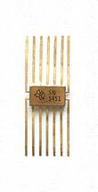
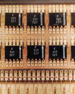
Flatpack is a US military standardized printed-circuit-board surface-mount-component package. The military standard MIL-STD-1835C defines: Flat package (FP). A rectangular or square package with leads parallel to base plane attached on two opposing sides of the package periphery.
The standard further defines different types with varying parameters which includes package body material, terminal location, package outline, lead form and terminal count.
The main vehicle for testing of high reliability flatpack packages has been MIL-PRF-38534 (General Specification for Hybrid Microcircuits). This document outlines the general requirements of fully assembled devices, whether they are single chip, multichip, or of hybrid technology. The test procedures of these requirements are found in MIL-STD-883 (Test Methods and Procedures for Microelectronics) as a listing of test methods. These methods cover various aspects of the minimum requirements that a microelectronics device must be able to attain before it is considered a compliant device.
History

The original flatpack was invented by Y. Tao in 1962 while he was working for Texas Instruments to improve heat dissipation. The dual in-line package was invented two years later. The first devices measured 1/4 inch by 1/8 inch (3.2 mm by 6.4 mm) and had 10 leads.[1]
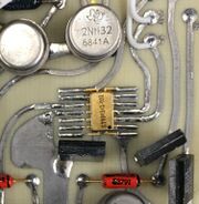
The flat package was smaller and lighter than the round TO-5 style transistor packages previously used for integrated circuits. Round packages were limited to 10 leads. Integrated circuits needed more leads to take full advantage of increasing device density. Since flat packages were made of glass, ceramic and metal, they could provide hermetic seals for circuits, protecting them from moisture and corrosion. Flat packs remained popular for military and aerospace applications long after plastic packages became standard for other application areas.
See also
References
- ↑ Dummer, G.W.A. Electronic Inventions and Discoveries 2nd ed. Pergamon Press ISBN 0-08-022730-9
 |
