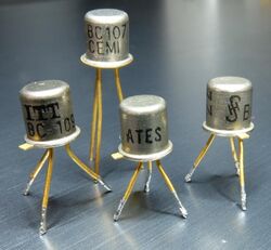
Engineering:TO-18

In electronics, TO-18 is a designation for a style of transistor metal case. The case is more expensive than the similarly sized plastic TO-92 package. The name is from JEDEC, signifying Transistor Outline Package, Case Style 18.[1]
Construction and orientation
The typical TO-18 metal can package has a base diameter of 5.6 mm (0.22 in), a cap diameter of 4.70 mm (0.185 in), a cap height of 4.83 mm (0.190 in).[1] The tab is located 45° from pin 1, which is typically the emitter. The lead diameter is nominally 0.45 mm (0.018 in). The leads are arranged in a circle with a diameter of 2.54 mm (0.100 in). The minimum length of the leads is 12.7 mm (0.50 in).
Different manufacturers have different tolerances, and the actual form factor may vary slightly, depending on function.
Uses and variants
The 3-lead TO-18 is used for transistors and other devices using no more than three leads. Variants for diodes, photodiodes and LEDs may have only two leads. Light-sensitive or light-emitting devices have a transparent window, lens, or parabolic reflectors in the top of the case rather than a sealed, flat top. For example, diode lasers such as those found in CD players may be packaged in TO-18 cases with a lens.
There are variants with between 2 and 8 leads.
TO-46 / TO-52
The TO-46[2] and TO-52[3] packages have 3 leads. These packages differ from all other variants in the height of the cap. Instead of 4.83 mm (0.190 in) the cap height is only 3.30 mm (0.130 in) for TO-52 and 1.90 mm (0.075 in) for TO-46.
TO-72
The package with 4 leads but otherwise with dimensions identical to TO-18, is standardized as TO-72.[4] The fourth wire is typically connected to the metal case as a means of electromagnetic shielding for radio frequency applications.
TO-71
The TO-71 package has 8 leads (up to three of those may be omitted).[5] The minimum angle between two adjacent leads is 45°.
TO-206
TO-206 is intended to replace previous definitions of packages with leads arranged in a circle with a diameter of 2.54 mm (0.100 in).[6][7] The different outlines are now defined as variants of TO-206: TO-18 is renamed to TO-206-AA, TO-46 to TO-206-AB, TO-52 to TO-206-AC, TO-72 to TO-206-AF. A new package with 3 leads and a cap height of 1.40 mm (0.055 in) (i.e. smaller than TO-46) is added as TO-206-AD. TO-206-AE does not require a minimum diameter of the leads but is otherwise identical to TO-18. The somewhat unrelated TO-58 package is included as TO-206-AG.
National standards
| Standards organization | Standard | Designation for | |||
|---|---|---|---|---|---|
| TO-18 | TO-46 | TO-71 | TO-72 | ||
| JEDEC | JEP95[7] | TO-206-AA | TO-206-AB | — | TO-206-AF |
| IEC | IEC 60191[lower-alpha 1][8] | C7/B11 | C10/B11 | C7/B12 | |
| DIN | DIN 41876[9][8] | 18A3 | 18A4 | ||
| EIAJ / JEITA | ED-7500A[lower-alpha 1][10] | TC-7/TB-8C, TC-7/TB-16C | — | — | TC-7/TB-9C |
| British Standards | BS 3934[lower-alpha 1][11][12] | SO-12A/SB3-6A | SO-12C/SB3-6A | SO-12A/SB8-1B | SO-12A/SB4-3 |
| Gosstandart | GOST 18472—88[13] | KT-1-7[lower-alpha 2] | KT-35-7[lower-alpha 3] | — | KT-1-12[lower-alpha 4] |
| Rosstandart | GOST R 57439[14] | ||||
| Kombinat Mikroelektronik Erfurt | TGL 11811[15] | A3/15-3a | — | — | A4/15-4a |
| TGL 26713/07[15] | F1BA3 | — | — | F1CA3 | |
See also
- Common transistors in a TO-18 package: 2N2222, BC108 family
- Common integrated circuits in a TO-18 package: ZN414
References
- ↑ 1.0 1.1 "JEDEC TO-18 package specification". Archived from the original on June 18, 2017. https://web.archive.org/web/20170618135128/https://www.jedec.org/sites/default/files/docs/archive/to/to-018.pdf.
- ↑ "TO-46". http://www.jedec.org/sites/default/files/docs/archive/to/to-046.pdf. Retrieved 2021-06-28.
- ↑ "TO-52". http://www.jedec.org/sites/default/files/docs/archive/to/to-052.pdf. Retrieved 2021-06-28.
- ↑ "TO-72". http://www.jedec.org/sites/default/files/docs/archive/to/to-072.pdf. Retrieved 2021-06-28.
- ↑ "TO-71". http://www.jedec.org/sites/default/files/docs/archive/to/to-071.pdf. Retrieved 2021-06-28.
- ↑ "Index by Device Type of Registered Transistor Outlines (TO)". JEDEC Publication No. 95. JEDEC. October 2010. https://www.jedec.org/sites/default/files/TOIND_DT.pdf. Retrieved 2021-07-13.
- ↑ 7.0 7.1 "Header Family 0.100 Pin Circle". JEDEC Publication No. 95. JEDEC. November 1982. pp. 182-185. https://www.jedec.org/system/files/docs/To-206b.pdf. Retrieved 2021-07-13.
- ↑ 8.0 8.1 "Semiconductors". Pro Electron. 1978. p. 215. https://datasheet.datasheetarchive.com/originals/scans/Scans-110/150.pdf. Retrieved 2021-06-17.
- ↑ "Semiconductor Databook". AEG-Telefunken. p. 15. https://datasheet.datasheetarchive.com/originals/scans/Scans-110/158.pdf. Retrieved 2021-08-20.
- ↑ "EIAJ ED-7500A Standards for the Dimensions of Semiconductor Devices". JEITA. 1996. https://home.jeita.or.jp/tsc/std-pdf/ED-7500A.pdf.
- ↑ "Semiconductor and Photoelectric Devices". Mullard. 1968. p. 467. https://frank.pocnet.net/other/Mullard/Mullard_Volume4PartIII_transistors_1968-11.pdf.
- ↑ "Mullard Technical Handbook Book 1 Part 1". Mullard. September 1974. p. 667. https://the-eye.eu/public/Books/Electronic%20Archive/MullardBook1Part11974_text.pdf.
- ↑ "ГОСТ 18472—88 ПРИБОРЫ ПОЛУПРОВОДНИКОВЫЕ - Основные размеры" (in ru). Rosstandart. 1988. p. 37-38. https://files.stroyinf.ru/Data2/1/4294834/4294834701.pdf.
- ↑ "ПРИБОРЫ ПОЛУПРОВОДНИКОВЫЕ - Основные размеры" (in ru). Rosstandart. 2017. p. 45. https://files.stroyinf.ru/Data/644/64413.pdf.
- ↑ 15.0 15.1 "TGL 26713/07: Gehäuse für Halbleiterbauelemente - Bauform F" (in de). Verlag für Standardisierung. June 1988. https://www.bbr-server.de/bauarchivddr/archiv/tglarchiv/tgl20001bis30000/tgl26501bis27000/tgl-26713-7-jun-1988.pdf. Retrieved 2021-06-15.
External links
- TO-18 Package, EESemi.com
 |


