Biology:SyNAPSE

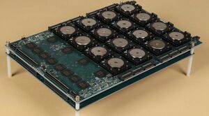
SyNAPSE is a DARPA program that aims to develop electronic neuromorphic machine technology, an attempt to build a new kind of cognitive computer with form, function, and architecture similar to the mammalian brain. Such artificial brains would be used in robots whose intelligence would scale with the size of the neural system in terms of the total number of neurons and synapses and their connectivity.
SyNAPSE is a backronym standing for Systems of Neuromorphic Adaptive Plastic Scalable Electronics. The name alludes to synapses, the junctions between biological neurons. The program is being undertaken by HRL Laboratories (HRL), Hewlett-Packard, and IBM Research. In November 2008, IBM and its collaborators were awarded $4.9 million in funding from DARPA while HRL and its collaborators were awarded $5.9 million in funding from DARPA. For the next phase of the project, DARPA added $16.1 million more to the IBM effort while HRL received an additional $10.7 million. In 2011, DARPA added $21 million more to the IBM project.[1] and an additional $17.9 million to the HRL project.[2] The SyNAPSE team for IBM is led by Dharmendra Modha, manager of IBM's cognitive computing initiative. The SyNAPSE team for HRL is led by Narayan Srinivasa, manager of HRL's Center for Neural and Emergent Systems.[3]
The initial phase of the SyNAPSE program developed nanometer scale electronic synaptic components capable of adapting the connection strength between two neurons in a manner analogous to that seen in biological systems (Hebbian learning), and simulated the utility of these synaptic components in core microcircuits that support the overall system architecture.
Continuing efforts will focus on hardware development through the stages of microcircuit development, fabrication process development, single chip system development, and multi-chip system development. In support of these hardware developments, the program seeks to develop increasingly capable architecture and design tools, very large-scale computer simulations of the neuromorphic electronic systems to inform the designers and validate the hardware prior to fabrication, and virtual environments for training and testing the simulated and hardware neuromorphic systems.
Published product highlights
- clockless operation (event-driven), consumes 70 mW during real-time operation, power density of 20 mW/cm2[4]
- manufactured in Samsung's 28 nm process technology, 5.4 billion transistors
- one million neurons and 256 million synapses networked into 4096 neurosynaptic cores by a 2D array, all programmable
- each core module integrates memory, computation, and communication, and operates in an event-driven, parallel, and fault-tolerant fashion
Participants
The following people and institutions are participating in the DARPA SyNAPSE program:[5]
IBM team, led by Dharmendra Modha
- Stanford University: Brian A. Wandell, H.-S. Philip Wong
- Cornell University: Rajit Manohar
- Columbia University Medical Center: Stefano Fusi
- University of Wisconsin–Madison: Giulio Tononi
- University of California, Merced: Christopher Kello
- iniLabs GmbH: Tobi Delbruck [6]
- IBM Research: Rajagopal Ananthanarayanan, Leland Chang, Daniel Friedman, Christoph Hagleitner, Bulent Kurdi, Chung Lam, Paul Maglio, Dharmendra Modha, Stuart Parkin, Bipin Rajendran, Raghavendra Singh
HRL Team led by Narayan Srinivasa
- HRL Laboratories: Narayan Srinivasa, Jose Cruz-Albrecht, Dana Wheeler, Tahir Hussain, Sri Satyanarayana, Tim Derosier, Youngkwan Cho, Corey Thibeault, Michael O' Brien, Michael Yung, Karl Dockendorf, Vincent De Sapio, Qin Jiang, Suhas Chelian
- Boston University: Massimiliano Versace, Stephen Grossberg, Gail Carpenter, Yongqiang Cao, Praveen Pilly
- Neurosciences Institute: Gerald Edelman, Einar Gall, Jason Fleischer
- University of Michigan: Wei Lu
- Georgia Institute of Technology: Jennifer Hasler
- University of California, Irvine: Jeff Krichmar
- George Mason University: Giorgio Ascoli, Alexei Samsonovich
- Portland State University: Christof Teuscher
- Stanford University: Mark Schnitzer
- Set Corporation: Chris Long
See also
- TrueNorth – IBM chip (introduced mid 2014) boasts of 1 million neurons and 256 million synapses (computing sense); 5.4 billion transistors and 4,096 neurosynaptic cores (hardware).
- Computational RAM is another approach bypassing the von Neumann bottleneck
References
- ↑ "I.B.M. Announces Brainy Computer Chip". The New York Times. 18 August 2011. http://bits.blogs.nytimes.com/2011/08/18/ibm-announces-brainy-computer-chip/?partner=rss&emc=rss. Retrieved 2015-03-31.
- ↑ "HRL Laboratories : HRL to Develop Neuromorphic Chip for Intelligent Machines in DARPA's SyNAPSE Program". Hrl.com. 2011-07-07. http://www.hrl.com/hrlDocs/pressreleases/2011/prsRls_110707.html. Retrieved 2015-03-31.
- ↑ "HRL Laboratories : Laboratories : CNES : Center for Neural & Emergent Systems". Hrl.com. 2015-02-26. http://www.hrl.com/laboratories/cnes/cnes_main.html. Retrieved 2015-03-31.
- ↑ New IBM SyNAPSE Chip Could Open Era of Vast Neural Networks IBM, August 7, 2014
- ↑ "Dharmendra S Modha's Cognitive Computing Blog: The Cat is Out of the Bag and BlueMatter". Modha.org. 2009-11-18. Archived from the original on 2015-04-02. https://web.archive.org/web/20150402095855/http://modha.org/blog/2009/11/post_3.html. Retrieved 2015-03-31.
- ↑ "IBM Research Creates New Foundation to Program SyNAPSE Chips". ibm.com. 2013-08-08. https://www-03.ibm.com/press/us/en/pressrelease/41710.wss. Retrieved 2015-06-09.
External links
- Systems of Neuromorphic Adaptive Plastic Scalable Electronics
- Neuromorphonics Lab, Boston University
- Center for Neural and Emergent Systems Homepage
- HRL Labs Homepage
 |

