Chemistry:Black silicon
Black silicon is a semiconductor material, a surface modification of silicon with very low reflectivity and correspondingly high absorption of visible (and infrared) light.
The modification was discovered in the 1980s as an unwanted side effect of reactive ion etching (RIE).[1][2] Other methods for forming a similar structure include electrochemical etching, stain etching, metal-assisted chemical etching, and laser treatment (which is developed in Eric Mazur's laboratory at Harvard University).
Black silicon has become a major asset to the solar photovoltaic industry as it enables greater light to electricity conversion efficiency[3] of standard crystalline silicon solar cells, which significantly reduces their costs.[4]
Properties


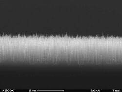
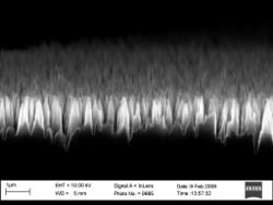
Black silicon is a needle-shaped surface structure where needles are made of single-crystal silicon and have a height above 10 µm and diameter less than 1 µm.[2] Its main feature is an increased absorption of incident light—the high reflectivity of the silicon, which is usually 20–30% for quasi-normal incidence, is reduced to about 5%. This is due to the formation of a so-called effective medium[5] by the needles. Within this medium, there is no sharp interface, but a continuous change of the refractive index that reduces Fresnel reflection. When the depth of the graded layer is roughly equal to the wavelength of light in silicon (about one-quarter the wavelength in vacuum) the reflection is reduced to 5%; deeper grades produce even blacker silicon.[6] For low reflectivity, the nanoscale features producing the index graded layer must be smaller than the wavelength of the incident light to avoid scattering.[6]

Applications
The unusual optical characteristics, combined with the semiconducting properties of silicon make this material interesting for sensor applications. Potential applications include:[7]
- Image sensors with increased sensitivity
- Thermal imaging cameras
- Photodetector with high-efficiency through increased absorption.[8][9]
- Mechanical contacts and interfaces[2]
- Terahertz applications.[10][11][12][13]
- Solar cells[14][15][16][17]
- Antibacterial surfaces[18] that work by physically rupturing bacteria's cellular membranes.
- Surface enhanced Raman spectroscopy[19]
- Ammonia Gas Sensors[20]
Production
Reactive-ion etching

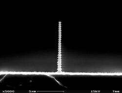
In semiconductor technology, reactive-ion etching (RIE) is a standard procedure for producing trenches and holes with a depth of up to several hundred micrometres and very high aspect ratios. In Bosch process RIE, this is achieved by repeatedly switching between an etching and passivation. With cryogenic RIE, the low temperature and oxygen gas achieve this sidewall passivation by forming SiO2, easily removed from the bottom by directional ions. Both RIE methods can produce black silicon, but the morphology of the resulting structure differs substantially. The switching between etching and passivation of the Bosch process creates undulated sidewalls, which are visible also on the black silicon formed this way.
During etching, however, small debris remain on the substrate; they mask the ion beam and produce structures that are not removed and in the following etching and passivation steps result in tall silicon pillars.[21] The process can be set so that a million needles are formed on an area of one square millimeter.[13]
Mazur's method
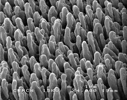
In 1999, a Harvard University group led by Eric Mazur developed a process in which black silicon was produced by irradiating silicon with femtosecond laser pulses.[22] After irradiation in the presence of a gas containing sulfur hexafluoride and other dopants, the surface of silicon develops a self-organized microscopic structure of micrometer-sized cones. The resulting material has many remarkable properties, such as absorption that extends to the infrared range, below the band gap of silicon, including wavelengths for which ordinary silicon is transparent. sulfur atoms are forced to the silicon surface, creating a structure with a lower band gap and therefore the ability to absorb longer wavelengths.

Similar surface modification can be achieved in vacuum using the same type of laser and laser processing conditions. In this case, the individual silicon cones lack sharp tips (see image). The reflectivity of such a micro-structured surface is very low, 3–14% in the spectral range 350–1150 nm.[23] Such reduction in reflectivity is contributed by the cone geometry, which increases the light internal reflections between them. Hence, the possibility of light absorption is increased. The gain in absorption achieved by fs laser texturization was superior to that achieved by using an alkaline chemical etch method,[24] which is a standard industrial approach for surface texturing of mono-crystalline silicon wafers in solar cell manufacturing. Such surface modification is independent of local crystalline orientation. A uniform texturing effect can be achieved across the surface of a multi-crystalline silicon wafer. The very steep angles lower the reflection to near zero and also increase the probability of recombination, keeping it from use in solar cells.
Nanopores
When a mix of copper nitrate, phosphorous acid, hydrogen fluoride and water are applied to a silicon wafer, the phosphorous acid reduction reduces the copper ions to copper nanoparticles. The nanoparticles attract electrons from the wafer's surface, oxidizing it and allowing the hydrogen fluoride to burn inverted pyramid-shaped nanopores into the silicon. The process produced pores as small as 590 nm that let through more than 99% of light.[25]
Chemical Etching
Black silicon can also be produced by chemical etching using a process called Metal-Assisted Chemical Etching (MACE).[26][27][28][29]
Function
When the material is biased by a small electric voltage, absorbed photons are able to excite dozens of electrons. The sensitivity of black silicon detectors is 100–500 times higher than that of untreated silicon (conventional silicon), in both the visible and infrared spectra.[30][31]
A group at the National Renewable Energy Laboratory reported black silicon solar cells with 18.2% efficiency.[17] This black silicon anti-reflective surface was formed by a metal-assisted etch process using nano particles of silver. In May 2015, researchers from Finland 's Aalto University, working with researchers from Universitat Politècnica de Catalunya announced they had created black silicon solar cells with 22.1% efficiency[32][33] by applying a thin passivating film on the nanostructures by Atomic Layer Deposition, and by integrating all metal contacts on the back side of the cell.
A team led by Elena Ivanova at Swinburne University of Technology in Melbourne discovered in 2012[34] that cicada wings were potent killers of Pseudomonas aeruginosa, an opportunist germ that also infects humans and is becoming resistant to antibiotics. The effect came from regularly-spaced "nanopillars" on which bacteria were sliced to shreds as they settled on the surface.
Both cicada wings and black silicon were put through their paces in a lab, and both were bactericidal. Smooth to human touch, the surfaces destroyed Gram-negative and Gram-positive bacteria, as well as bacterial spores.
The three targeted bacterial species were P. aeruginosa, Staphylococcus aureus and Bacillus subtilis, a wide-ranging soil germ that is a cousin of anthrax.
The killing rate was 450,000 bacteria per square centimetre per minute over the first three hours of exposure or 810 times the minimum dose needed to infect a person with S. aureus, and 77,400 times that of P. aeruginosa. However, it was later proven that the quantification protocol of Ivanova's team was not suitable for these kind of antibacterial surfaces.
See also
- Quantum efficiency of a solar cell
- Solasys
- University of Wisconsin-Madison. "'Stealth' material hides hot objects from infrared eyes." ScienceDaily. www.sciencedaily.com/releases/2018/06/180622174752.htm (accessed 23 June 2018).
References
- ↑ Jansen, H; Boer, M de; Legtenberg, R; Elwenspoek, M (1995). "The black silicon method: a universal method for determining the parameter setting of a fluorine-based reactive ion etcher in deep silicon trench etching with profile control". Journal of Micromechanics and Microengineering 5 (2): 115–120. doi:10.1088/0960-1317/5/2/015. Bibcode: 1995JMiMi...5..115J. https://research.utwente.nl/en/publications/the-black-silicon-method-a-universal-method-for-determining-the-parameter-setting-of-a-fluorinebased-reactive-ion-etcher-in-deep-silicon-trench-etching-with-profile-control(bd036618-f419-4d06-b9f7-190c94288bd9).html.
- ↑ 2.0 2.1 2.2 Black Silicon[yes|permanent dead link|dead link}}] as a functional layer of the micro-system technology
- ↑ Alcubilla, Ramon; Garín, Moises; Calle, Eric; Ortega, Pablo; Gastrow, Guillaume von; Repo, Päivikki; Savin, Hele (2015). "Black silicon solar cells with interdigitated back-contacts achieve 22.1% efficiency" (in en). Nature Nanotechnology 10 (7): 624–628. doi:10.1038/nnano.2015.89. ISSN 1748-3395. PMID 25984832. Bibcode: 2015NatNa..10..624S. https://aaltodoc.aalto.fi/handle/123456789/16406.
- ↑ Pearce, Joshua; Savin, Hele; Pasanen, Toni; Laine, Hannu; Modanese, Chiara; Modanese, Chiara; Laine, Hannu S.; Pasanen, Toni P. et al. (2018). "Economic Advantages of Dry-Etched Black Silicon in Passivated Emitter Rear Cell (PERC) Photovoltaic Manufacturing" (in en). Energies 11 (9): 2337. doi:10.3390/en11092337.
- ↑ C. Tuck Choy (1999). Effective Medium Theory: Principles and Applications. Oxford University Press. ISBN 978-0-19-851892-1. https://books.google.com/books?id=SK_Jn3YwAu4C.
- ↑ 6.0 6.1 Branz, H.M.; Yost, V.E.; Ward, S.; To, B.; Jones, K.; Stradins, P. (2009). "Nanostructured black silicon and the optical reflectance of graded-density surfaces". Appl. Phys. Lett. 94 (23): 231121–3. doi:10.1063/1.3152244. Bibcode: 2009ApPhL..94w1121B. https://zenodo.org/record/1232047.
- ↑ Carsten Meyer: "Black Silicon: sensor material of the future?" Heise Online. 5 February 2009
- ↑ Koynov, Svetoslav; Brandt, Martin S.; Stutzmann, Martin (2006). "Black nonreflecting silicon surfaces for solar cells". Applied Physics Letters 88 (20): 203107. doi:10.1063/1.2204573. Bibcode: 2006ApPhL..88t3107K. http://www.wsi.tum.de/Portals/0/media/e25/brandt/pdfs/apl_koynov_nonreflecting.pdf.
- ↑ Koynov, Svetoslav; Brandt, Martin S.; Stutzmann, Martin (2007). "Black multi-crystalline silicon solar cells". Physica Status Solidi RRL 1 (2): R53. doi:10.1002/pssr.200600064. Bibcode: 2007PSSRR...1R..53K. http://www.wsi.tum.de/Portals/0/media/e25/brandt/pdfs/pss_koynov_black_mukticrystalline.pdf.
- ↑ Gail Overton: Terahertz Technology: Black silicon emits terahertz radiation. In:Laser Focus World, 2008
- ↑ Cheng-Hsien Liu: Formation of Silicon nanopores and Nanopillars by a Maskless Deep Reactive Ion Etching Process [yes|permanent dead link|dead link}}], 11 November 2008
- ↑ Zhiyong Xiao (2007). "Formation of Silicon Nanopores and Nanopillars by a Maskless Deep Reactive Ion Etching Process". TRANSDUCERS 2007 – 2007 International Solid-State Sensors, Actuators and Microsystems Conference—Formation of Silicon Nanopores and Nanopillars by a Maskless Deep Reactive Ion Etching Process. pp. 89–92. doi:10.1109/SENSOR.2007.4300078. ISBN 978-1-4244-0841-2.
- ↑ 13.0 13.1 Martin Schaefer: Velcro in miniature – "silicon grass holds together micro-components" In: wissenschaft.de. 21 June 2006.
- ↑ Branz, Howard M.; Yuan, Hao-Chih; Oh, Jihun (2012). "An 18.2%-efficient black-silicon solar cell achieved through control of carrier recombination in nanostructures" (in en). Nature Nanotechnology 7 (11): 743–748. doi:10.1038/nnano.2012.166. ISSN 1748-3395. PMID 23023643. Bibcode: 2012NatNa...7..743O.
- ↑ Liu, Xiaogang; Coxon, Paul; Peters, Marius; Hoex, Bram; Cole, Jacqueline; Fray, Derek (2014). "Black silicon: fabrication methods, properties and solar energy applications". Energy & Environmental Science 7 (10): 3223–3263. doi:10.1039/C4EE01152J.
- ↑ Black Silicon Comes Back – And Cheaper than Ever, 7 September 2010
- ↑ 17.0 17.1 Oh, J.; Yuan, H.-C.; Branz, H.M. (2012). "Carrier recombination mechanisms in high surface area nanostructured solar cells by study of 18.2%-efficient black silicon solar cells". Nature Nanotechnology 7 (11): 743–8. doi:10.1038/nnano.2012.166. PMID 23023643. Bibcode: 2012NatNa...7..743O.
- ↑ "Black silicon slices and dices bacteria". Gizmag.com. http://www.gizmag.com/black-silicon-antibacterial-surface/29950/.
- ↑ Xu, Zhida; Jiang, Jing; Gartia, Manas; Liu, Logan (2012). "Monolithic Integrations of Slanted Silicon Nanostructures on 3D Microstructures and Their Application to Surface-Enhanced Raman Spectroscopy". The Journal of Physical Chemistry C 116 (45): 24161–24170. doi:10.1021/jp308162c.
- ↑ Liu, Xiao-Long; Zhu, Su-Wan; Sun, Hai-Bin; Hu, Yue; Ma, Sheng-Xiang; Ning, Xi-Jing; Zhao, Li; Zhuang, Jun (17 January 2018). ""Infinite Sensitivity" of Black Silicon Ammonia Sensor Achieved by Optical and Electric Dual Drives". ACS Appl. Mater. Interfaces 10 (5): 5061–5071. doi:10.1021/acsami.7b16542. PMID 29338182.
- ↑ Mike Stubenrauch, Martin Hoffmann, Siliziumtiefätzen (DRIE)[yes|permanent dead link|dead link}}], 2006
- ↑ William J. Cromie arises:Black Silicon, A New Way To Trap Light .In:Harvard Gazette.9 December 1999, accessed on 16 February 2009.
- ↑ Torres, R., Vervisch, V., Halbwax, M., Sarnet, T., Delaporte, P., Sentis, M., Ferreira, J., Barakel, D., Bastide, S., Torregrosa, F., Etienne, H., and Roux, L., "Femtosecond laser texturization for improvement of photovoltaic cells: Black silicon", Journal of Optoelectronics and Advanced Materials, Volume 12, No. 3, pp. 621–625, 2010.
- ↑ Sarnet, T., Torres, R., Vervisch, V., Delaporte, P., Sentis, M., Halbwax, M., Ferreira, J., Barakel, D., Pasquielli, M., Martinuzzi, S., Escoubas, L., Torregrosa, F., Etienne, H., and Roux, L., "Black silicon recent improvements for photovaltaic cells", Proceedings of the International Congress on Applications of Lasers & Electro-Optics, 2008.
- ↑ Williams, Mike (2014-06-18). "One step to solar cell efficiency". Rdmag.com. http://www.rdmag.com/news/2014/06/one-step-solar-cell-efficiency?et_cid=4005000&et_rid=677699018&location=top.
- ↑ Hsu, Chih-Hung; Wu, Jia-Ren; Lu, Yen-Tien; Flood, Dennis J.; Barron, Andrew R.; Chen, Lung-Chien (2014-09-01). "Fabrication and characteristics of black silicon for solar cell applications: An overview" (in en). Materials Science in Semiconductor Processing 25: 2–17. doi:10.1016/j.mssp.2014.02.005. ISSN 1369-8001.
- ↑ Koynov, Svetoslav; Brandt, Martin S.; Stutzmann, Martin (2007). "Black multi-crystalline silicon solar cells" (in en). Physica Status Solidi RRL 1 (2): R53–R55. doi:10.1002/pssr.200600064. ISSN 1862-6270. Bibcode: 2007PSSRR...1R..53K.
- ↑ Chen, Kexun; Zha, Jiawei; Hu, Fenqin; Ye, Xiaoya; Zou, Shuai; Vähänissi, Ville; Pearce, Joshua M.; Savin, Hele et al. (2019-03-01). "MACE nano-texture process applicable for both single- and multi-crystalline diamond-wire sawn Si solar cells" (in en). Solar Energy Materials and Solar Cells 191: 1–8. doi:10.1016/j.solmat.2018.10.015. ISSN 0927-0248. https://hal.archives-ouvertes.fr/hal-02111354/file/MACE_nano-texture_process_applicable_for.pdf.
- ↑ Uddin, Shahnawaz; Hashim, Md. Roslan; Pakhuruddin, Mohd Zamir (2021-03-12). "Aluminium-assisted chemical etching for fabrication of black silicon" (in en). Materials Chemistry and Physics 124469: 124469. doi:10.1016/j.matchemphys.2021.124469. ISSN 0254-0584.
- ↑ Wade Roush: "SiOnyx Brings "Black Silicon" into the Light; Material Could upend Solar, Imaging Industries". In: Xconomy. 10 December 2008
- ↑ 'Black Silicon' A new type of silicon promises cheaper, more-sensitive light detectors, Technology Review Online. 29 October 2008
- ↑ "Efficiency record for black silicon solar cells jumps to 22.1%". https://www.sciencedaily.com/releases/2015/05/150518121440.htm.
- ↑ Savin, Hele; Repo, Päivikki; von Gastrow, Guillaume; Ortega, Pablo; Calle, Eric; Garín, Moises; Alcubilla, Ramon (2015). "Black silicon solar cells with interdigitated back-contacts achieve 22.1% efficiency". Nature Nanotechnology 10 (7): 624–628. doi:10.1038/nnano.2015.89. PMID 25984832. Bibcode: 2015NatNa..10..624S. https://aaltodoc.aalto.fi/handle/123456789/16406.
- ↑ Elena P. Ivanova; Jafar Hasan; Hayden K. Web; Vi Khanh Truon; Gregory S. Watson; Jolanta A. Watson; Vladimir A. Baulin; Sergey Pogodin et al. (20 August 2012). "Natural Bactericidal Surfaces: Mechanical Rupture of Pseudomonas aeruginosa Cells by Cicada Wings". Small 8 (17): 2489–2494. doi:10.1002/smll.201200528. PMID 22674670.
External links
- SiOnyx brings "Black Silicon" into the light
- New New York Times article (needs NYT subscription)[yes|permanent dead link|dead link}}]
- SiOnyx homepage
- Lasers for Photovoltaics – Knowledge Base
- E. Mazur; J. Carey; C. Crouch; R. Younkins (2001). "Fabrication of micrometer-sized conical field emitters using femtosecond laser-assisted etching of silicon". MRS Spring Meeting. http://mazur.harvard.edu/publications/Pub_287.pdf. Retrieved 6 March 2015.
- Lasers Improve PV Efficiency
- Lasers, Plasmas et Procédés Photoniques – Recherche – Structuration du silicium : Application au Photovoltaïque (in French)

