Chemistry:Marchywka effect

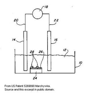
The Marchywka effect[2][3] refers to electrochemical cleaning of diamond using an electric field induced with remote electrodes.
Discovery and development
It was first observed by accident by Mike Marchywka[1] while trying to find a selective means to etch non-diamond carbon and fabricate simple astronomical UV detection devices.[4] These devices required a few specific features such as clean surfaces and patterned areas of non-diamond carbon but the approach has subsequently been explored as a more general means to terminate carbon surfaces and selectively clean and etch various other materials or structures. The term "Marchywka effect" is not used consistently and sometimes the term "bipolar surface treatment" is used[5] as the substrate is induced to become a bipolar electrode.[6] Various phrases such as "non-contacted electrochemical" process may also be used (see any references cited herein) or it may be mentioned as just an "electrochemical etch".[7][8]
While this is easily confused with various common electrochemical cells, and may appear to be a trivial and obvious extension of well known methods, recent patents[9] continue to reference prior work[10] that cites non-contactedness as a feature. The use of a low conductivity medium as used in Marchywka et al.'s original paper[4] is sometimes noted when it is used and may produce new effects.[11][12] The apparatus to create the effect is similar to the well-known electroporation system except that the biological specimen is replaced with an inorganic substrate,[4] although, in some cases, organic films can be etched with this process using a surfactant solution as the electrolyte.
Surface effects

As a "non-contact" process, the effect differs from traditional electrochemical processes where carrier flow through the surface is achieved by connection to a current source with highly conductive materials such as copper wire. It is well known[by whom?] that materials contacted to an anode can be modified in a variety of ways including anodizing and electropolishing. Electrochemistry was quickly recognized as an important related field in the popular press once the first synthetic diamonds were made.[14] However, the use of an induced field created by remote electrodes allows discontinuous areas on an insulating substrate to be cleaned, modified, or etched (similar to electroetching), greatly expanding the role of electrochemical methods.
The mechanism is presumed to be due to the induced field but little in the way of exhaustive analysis has been done, as the actual processes do not appear to differ from traditional approaches. For example, "identified as the ‘Marchywka Effect’ in the literature. The etching may be due to the galvanic coupling of diamond and non-diamond carbon".[15] The applied field apparently creates directed surface modifications on polished diamond surfaces with little or no actual removal of material. This may be desirable for making various devices, or simply studying the properties of the diamond surface. The induced field deposits or replaces a single layer of some molecule and this could be thought of as a monolayer electroplating method. It has been elucidated in more fully in many works.[16][17]
Earlier related approaches

Many prior technologies exist for preparing wide-gap diamond for use in electronic devices or as a substrate for single-crystal diamond growth. The more stable forms of carbon have lower gaps and different crystal structures, and their presence must be carefully controlled. The Marchywka Effect has been characterised and compared to alternative means to create a desired surface for several applications.
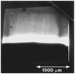
Removal of non-diamond carbon with wet chemicals had been accomplished by boiling in mixtures of sulfuric and chromic acid. When applied to a diamond substrate with an ion implantation damage profile as may be used for basic science, crystal growth, or device fabrication,[18][19] the electrochemical approach makes it easier to preserve the thin film of less damaged diamond lying above the implant range, and it has been used in annealing experiments to fix the diamond after implantation damage has occurred.[20] In some cases, thermal cycling may be an issue and selectivity to various masks may be important, so the lower temperatures and more flexible chemistry may offer benefits over prior art.
The method does not require the use of non-volatile materials[citation needed] such as chrome, possibly reducing contamination problems in some applications. The ability to control the etching direction and speed with an applied voltage or electrode configuration, as with electrochemical machining, gives additional capabilities not available with isotropic chemical-only approaches. Dry processing methods such as hot oxygen or plasmas can also burn off the graphite faster than the diamond, as can a simple acetylene torch. These require higher temperatures and do not have the same high selectivity that can be achieved with the electrochemical approach.[21]
Surface termination is often an issue with both solid state and vacuum devices, and the details of final surface band structure have been compared with alternatives in various device structures.[22] [23]
Applications
While the original effort failed to produce useful products, follow-on work in Europe did produce usable astronomical detectors[24] [25] but without apparent use of this technology. In other areas, however, the approach seems to be competitive, with prior art for making various end-products, since it has been used as a fabrication step for experimental devices and structures. Many groups have used the approach to grow homoepitaxial diamond[citation needed] and subsequently release the thin-films with a variety of "lift-off" processes.[26]
It has also been considered in contexts such as carbon microelectromechanical systems production[27][28] and different materials applications, for example with non-contacted palladium[6][29] deposition and extensions.[9] While not citing Marchywka et al.'s original paper, these continue to cite non-contactedness as a feature, "The electrode assembly and the conductive surface may be positioned in close proximity to, but without contacting, one another".[9] references a much earlier patent[10] covering related attempts to achieve non-contacted electro-etching, "The present invention relates to a method of and apparatus for electrochemically processing metallic surfaces of workpieces arranged in a contact-free manner with regard to the cathode and anode[...]."[4]
The effect has been mentioned in passing with regard to novel devices such as quantum coherent devices[30] while patents on emerging uses for amorphous carbon [31] [32] and diamond thermal conductors[33] by manufacturers of high density electronic chips reference the related lift-off technology.
See also
References
- ↑ 1.0 1.1 United States Patent Number 5269890
- ↑ Pan, LS; Kania DR(1995). "Diamond: Electronic Properties and Applications" p 43 (Springer) ISBN 0-7923-9524-7, ISBN 978-0-7923-9524-9
- ↑ Pearton, SJ (2000)."Wide Bandgap Semiconductors: Growth, Processing and Applications" pg. 525. (William Andrew Inc.); ISBN 0-8155-1439-5, ISBN 978-0-8155-1439-8
- ↑ 4.0 4.1 4.2 4.3 Marchywka, MJ; Pehrsson, PE; Binari, SC; Moses, DJ (February 1993). "Electrochemical Patterning of Amorphous Carbon on Diamond". Journal of the Electrochemical Society 140 (2): L19–L22. doi:10.1149/1.2221093. Bibcode: 1993JElS..140L..19M. full text
- ↑ Pleskov, YV "The Electrochemistry of Diamond" in Alkire, RC; Kolb, DM ed(2003). Advances In Electrochemical Science and Engineering pg 224 (Wiley-VCH). ISBN 3527302115, ISBN 978-3-527-30211-6
- ↑ 6.0 6.1 Bradley, JC; Ma, Z (1999). "Contactless Electrodeposition of Palladium Catalysts". Angew. Chem. Int. Ed. Engl. 38 (11): 1663–1666. doi:10.1002/(SICI)1521-3773(19990601)38:11<1663::AID-ANIE1663>3.0.CO;2-C. PMID 29710991. http://www.drexel.edu/coas/chemistry/Faculty%20PDFs/2008-09%20Faculty%20Publications%20List.pdf.
- ↑ Jaeger, MD; et., al; Day, A. R.; Thorpe, M. F.; Golding, B. (May 11, 1998). "Resistivity of boron-doped diamond microcrystals". Applied Physics Letters 72 (19): 2445. doi:10.1063/1.121680. Bibcode: 1998ApPhL..72.2445J. http://biophysics.asu.edu/thorpe/publications/196.pdf.
- ↑ D'Evelyn MP "Surface Properties of Diamond" in Prelas, Popovici, Bigelow ed(1997). Handbook of Industrial Diamonds and Diamond Films (CRC Press). ISBN 0824799941, ISBN 978-0-8247-9994-6
- ↑ 9.0 9.1 9.2 United States Patent Number 7435324
- ↑ 10.0 10.1 United States Patent Number 4153531
- ↑ Bradley, JC; et., al; Crawford, Jeffrey; Eckert, Jennifer; Ernazarova, Karima; Kurzeja, Thomas; Lin, Muduo; McGee, Michael et al. (September 18, 1997). "Creating electrical contacts between metal particles using directed electrochemical growth". Nature 389 (6648): 268–271. doi:10.1038/38464. Bibcode: 1997Natur.389..268B.
- ↑ Fleischmann, Martin; Ghoroghchian, Jamal; Rolison, Debra; Pons, Stanley (September 18, 1986). "Electrochemical Dispersions of Spherical Ultramicroelectrodes". J. Phys. Chem. 90 (23): 6392–6400. doi:10.1021/j100281a065. http://www.dtic.mil/get-tr-doc/pdf?AD=ADA193493.
- ↑ 13.0 13.1 Marchywka, MJ; Pehrsson, PE; Moses, D; Pehrsson, PE; Moses, DJ (May 1993). "Electrochemical Patterning of Amorphous Carbon on Diamond.". in Diismukes. Honolulu: ECS. pp. 626–631. ISBN 9781566770606. https://books.google.com/books?id=vEGZ9loshAsC&q=marchywka+hawaii&pg=PR5.
- ↑ Kaempffert, W (May 22, 1955). "High Pressures and High Temperatures Open New World in Electrochemistry". New York Times: E9. http://select.nytimes.com/gst/abstract.html?res=F10A14F63B5410718EDDAB0A94DD405B8589F1D3.
- ↑ Ramesham, R (March 1998). "Effect of annealing and hydrogen plasma treatment on the voltammetric and impedance behavior of the diamond electrode". Thin Solid Films 315 (2): 222–228. doi:10.1016/S0040-6090(97)00592-0. Bibcode: 1998TSF...315..222R.
- ↑ 16.0 16.1 16.2 Pehrsson, PE; Long, JP; Marchywka, MJ; Butler, JE (December 1995). "Electrochemically induced surface chemistry and negative electron affinity on diamond (100)". Appl. Phys. Lett. 67 (23): 3414. doi:10.1063/1.115264. Bibcode: 1995ApPhL..67.3414P. http://link.aip.org/link/?APPLAB/67/3414/1. Retrieved 2019-05-05. full text
- ↑ Szunerits, Sabine; Boukherroub, Rabah (2008). "Different strategies for functionalization of diamond surfaces". J Solid State Electrochem 12 (10): 1205–1218. doi:10.1007/s10008-007-0473-3.
- ↑ Prins, JF (2003). "Ion implantation of diamond for electronic applications". Semicond. Sci. Technol. 18 (3): S27–S33. doi:10.1088/0268-1242/18/3/304. Bibcode: 2003SeScT..18S..27P.
- ↑ United States Patent Number 5385762
- ↑ Lai, PF; Prawer, S; Bursill, LA (Jan 2001). "Recovery of diamond after irradiation at high energy and annealing". Diamond and Related Materials 10 (1): 82–86. doi:10.1016/S0925-9635(00)00406-4. Bibcode: 2001DRM....10...82L.
- ↑ Baumann, PK (1998). "Surface cleaning, electronic states and electron affinity of diamond(100), (111) and (110) surfaces". Surface Science 409 (2): 320–335. doi:10.1016/S0039-6028(98)00259-3. Bibcode: 1998SurSc.409..320B. http://cat.inist.fr/?aModele=afficheN&cpsidt=2339856.
- ↑ Characterization of cobalt-diamond (100) interfaces: electron affinity and Schottky barrier
- ↑ Baumann, PK; Nemanich, RJ (1996). "Characterization of cobalt-diamond (100) interfaces: electron affinity and Schottky barrier". Applied Surface Science 104–105 (2): 267–273. doi:10.1016/S0169-4332(96)00156-0. Bibcode: 1996ApSS..104..267B.
- ↑ Hochedez publication list
- ↑ Marchywka, M; Hochedez, JF; Geis, MW; Socker, DG; Moses, D; Goldberg, RT (1991). "Ultraviolet photoresponse characteristics of diamond diodes". Applied Optics 30 (34): 5011–5013. doi:10.1364/AO.30.005011. PMID 20717311. Bibcode: 1991ApOpt..30.5011M. http://www.opticsinfobase.org/ao/abstract.cfm?uri=ao-30-34-5011.
- ↑ Butler, JE (Spring 2003). "CVD Diamond: Maturity and Diversity". Electrochemical Society Interface: 22–26. http://www.electrochem.org/dl/interface/spr/spr03/IF3-03-Pages22-26.pdf.
- ↑ Wang, CF; Hu, EL; Yang, J.; Butler, J. E. (May 2007). "Fabrication of suspended single crystal diamond devices by electrochemical etch". Journal of Vacuum Science & Technology B: Microelectronics and Nanometer Structures 25 (3): 730–733. doi:10.1116/1.2731327. Bibcode: 2007JVSTB..25..730W.
- ↑ Zalalutdinov, MK; Baldwin, JW; Pate, BB; Yang, J; Butler, JE; Houston, BH (May 2008). "Single Crystal Diamond Nanomechanical Dome Resonator". NRL Review Nanoscience Technology: 190–191. https://www.nrl.navy.mil/content_images/08Nano_Zalalutdinov.pdf.
- ↑ Bradley, JC; Zhongming, M (1999). "Berührungsloses elektrolytisches Abscheiden von Palladiumkatalysatoren". Angewandte Chemie 111 (11): 1768–1771. doi:10.1002/(SICI)1521-3757(19990601)111:11<1768::AID-ANGE1768>3.0.CO;2-#.
- ↑ Greentree, Andrew; Olivero, Paolo; Draganski, Martin; Trajkov, Elizabeth; Rabeau, James R; Reichart, Patrick; Gibson, Brant C; Rubanov, Sergey et al. (May 2006). "Critical components for diamond-based quantum coherent devices". J. Phys.: Condens. Matter 18 (21): S825–S842. doi:10.1088/0953-8984/18/21/S09. Bibcode: 2006JPCM...18S.825G. http://www.qcaustralia.org/Publications/2006/Greentree_Olivero_et%20al.pdf.
- ↑ United States Patent Number 7521304
- ↑ United States Patent Number 7084071
- ↑ United States Patent Number 7501330
External links
- Scirus Search Results
- Recent Related Patents
- Recent Citations that may reference Marchywka Effect[|permanent dead link|dead link}}]
