Engineering:Π pad
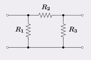
The Π pad (pi pad) is a specific type of attenuator circuit in electronics whereby the topology of the circuit is formed in the shape of the Greek capital letter pi (Π).
Attenuators are used in electronics to reduce the level of a signal. They are also referred to as pads due to their effect of padding down a signal by analogy with acoustics. Attenuators have a flat frequency response attenuating all frequencies equally in the band they are intended to operate. The attenuator has the opposite task of an amplifier. The topology of an attenuator circuit will usually follow one of the simple filter sections. However, there is no need for more complex circuitry, as there is with filters, due to the simplicity of the frequency response required.
Circuits are required to be balanced or unbalanced depending on the geometry of the transmission lines with which they are to be used. For radio frequency applications, the format is often unbalanced, such as coaxial. For audio and telecommunications, balanced circuits are usually required, such as with the twisted pair format. The Π pad is intrinsically an unbalanced circuit. However, it can be converted to a balanced circuit by placing half the series resistance in the return path. Such a circuit is called a box section because the circuit is formed in the shape of a box.
Terminology
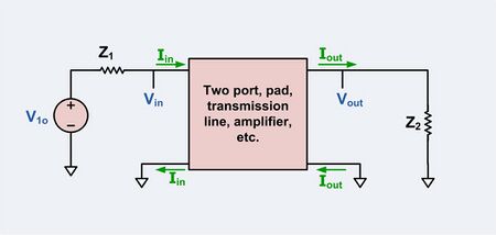
An attenuator is a form of a two-port network with a generator connected to one port and a load connected to the other. In all of the circuits given below it is assumed that the generator and load impedances are purely resistive (though not necessarily equal) and that the attenuator circuit is required to perfectly match to these. The symbols used for these impedances are;
- the impedance of the generator
- the impedance of the load
Popular values of impedance are 600Ω in telecommunications and audio, 75Ω for video and dipole antennae, and 50Ω for RF.
The voltage transfer function, A, is,
While the inverse of this is the loss, L, of the attenuator,
The value of attenuation is normally marked on the attenuator as its loss, LdB, in decibels (dB). The relationship with L is;
Popular values of attenuator are 3dB, 6dB, 10dB, 20dB, and 40dB.
However, it is often more convenient to express the loss in nepers,
where is the attenuation in nepers (one neper is approximately 8.7 dB).
Impedance and loss
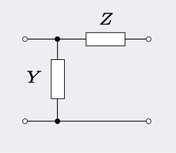
The values of resistance of the attenuator's elements can be calculated using image parameter theory. The starting point here is the image impedances of the L section in figure 2. The image admittance of the input is,
and the image impedance of the output is,
The loss of the L section when terminated in its image impedances is,
where the image parameter transmission function, γL is given by,
The loss of this L section in the reverse direction is given by,
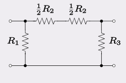
For an attenuator, Z and Y are simple resistors and γ becomes the image parameter attenuation (that is, the attenuation when terminated with the image impedances) in nepers. A Π pad can be viewed as being two L sections back-to-back as shown in figure 3. Most commonly, the generator and load impedances are equal so that Z1 = Z2 = Z0 and a symmetrical Π pad is used. In this case, the impedance matching terms inside the square roots all cancel and,
Substituting Z and Y for the corresponding resistors,
These equations can easily be extended to non-symmetrical cases.
Resistor values
The equations above find the impedance and loss for an attenuator with given resistor values. The usual requirement in a design is the other way around – the resistor values for a given impedance and loss are needed. These can be found by transposing and substituting the last two equations above;
- If
- with
O pad
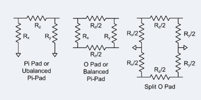
The unbalanced pi pad can be converted to a balanced O pad by putting one half of Rz in each side of a balanced line.
The simple four element O pad attenuates the differential mode signal but does little to attenuate any common mode signal. To insure attenuation of the common mode signal also, a split O pad can be created by splitting and grounding Rx and Ry.
Conversion of two-port to pi pad

If a passive two-port can be expressed with admittance parameters, then that two-port is equivalent to a pi pad. In general, the admittance parameters are frequency dependent and not necessarily resistive. In that case the elements of the pi pad would not be simple components. However, in the case where the two-port is purely resistive or substantially resistive over the frequency range of interest, then the two-port can be replaced with a pi pad made of resistors.
Conversion of tee pad to pi pad
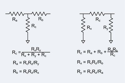
Pi pads and tee pads are easily converted back and forth.
If one of the pads is composed of only resistors then the other is also composed entirely of resistors.
See also
References
- Matthaei, Young, Jones, Microwave Filters, Impedance-Matching Networks, and Coupling Structures, pp. 41–45, 4McGraw-Hill 1964.
- Redifon Radio Diary, 1970, pp. 49–60, William Collins Sons & Co, 1969.
 |
