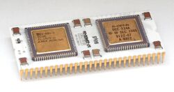
Engineering:Hybrid integrated circuit

A hybrid integrated circuit (HIC), hybrid microcircuit, hybrid circuit or simply hybrid is a miniaturized electronic circuit constructed of individual devices, such as semiconductor devices (e.g. transistors, diodes or monolithic ICs) and passive components (e.g. resistors, inductors, transformers, and capacitors), bonded to a substrate or printed circuit board (PCB).[1] A PCB having components on a Printed wiring board (PWB) is not considered a true hybrid circuit according to the definition of MIL-PRF-38534.
Overview
"Integrated circuit", as the term is currently used, usually refers to a monolithic IC which differs notably from a HIC in that a HIC is fabricated by inter-connecting a number of components on a substrate whereas an IC's (monolithic) components are fabricated in a series of steps entirely on a single wafer which is then diced into chips.[2] Some hybrid circuits may contain monolithic ICs, particularly Multi-chip module (MCM) hybrid circuits.

Hybrid circuits could be encapsulated in epoxy, as shown in the photo, or in military and space applications, a lid was soldered onto the package. A hybrid circuit serves as a component on a PCB in the same way as a monolithic integrated circuit; the difference between the two types of devices is in how they are constructed and manufactured. The advantage of hybrid circuits is that components which cannot be included in a monolithic IC can be used, e.g., capacitors of large value, wound components, crystals, inductors.[3] In military and space applications, numerous integrated circuits, transistors and diodes, in their die form, would be placed on either a ceramic or beryllium substrate. Either gold or aluminum wire would be bonded from the pads of the IC, transistor, or diode to the substrate.
Thick film technology is often used as the interconnecting medium for hybrid integrated circuits. The use of screen printed thick film interconnect provides advantages of versatility over thin film although feature sizes may be larger and deposited resistors wider in tolerance. Multi-layer thick film is a technique for further improvements in integration using a screen printed insulating dielectric to ensure connections between layers are made only where required. One key advantage for the circuit designer is complete freedom in the choice of resistor value in thick film technology. Planar resistors are also screen printed and included in the thick film interconnect design. The composition and dimensions of resistors can be selected to provide the desired values. The final resistor value is determined by design and can be adjusted by laser trimming. Once the hybrid circuit is fully populated with components, fine tuning prior to final test may be achieved by active laser trimming.


Thin film technology was also employed in the 1960s. Ultra Electronics manufactured circuits using a silica glass substrate. A film of tantalum was deposited by sputtering followed by a layer of gold by evaporation. The gold layer was first etched following the application of a photoresist to form solder compatible connection pads. Resistive networks were formed, also by a photoresist and etching process. These were trimmed to a high precision by selective adonization of the film. Capacitors and semiconductors were in the form of LID (Leadless Inverted Devices) soldered to the surface by selectively heating the substrate from the underside. Completed circuits were potted in a diallyl phthalate resin. Several customized passive networks were made using these techniques as were some amplifiers and other specialized circuits. It is believed that some passive networks were used in the engine control units manufactured by Ultra Electronics for Concorde.
Some modern hybrid circuit technologies, such as LTCC-substrate hybrids, allow for embedding of components within the layers of a multi-layer substrate in addition to components placed on the surface of the substrate. This technology produces a circuit that is, to some degree, three-dimensional.

Hybrid ICs are especially suitable for analog signals. They were used in some early digital computers but were replaced therein by monolithic ICs which offered higher performance.[4][5][6]
Other electronic hybrids
In the early days of telephones, separate modules containing transformers and resistors were called hybrids or hybrid coils; they have been replaced by semiconductor integrated circuits.
In the early days of transistors the term hybrid circuit was used to describe circuits with both transistors and vacuum tubes; e.g., an audio amplifier with transistors used for voltage amplification followed by a vacuum tube power output stage, as suitable power transistors were not available. This usage, and the devices, are obsolete, however amplifiers that use a tube preamplifier stage coupled with a solid state output stage are still in production, and are called hybrid amplifiers in reference to this.
See also
- Chip on board, aka black blobs
- System in a package
- Multi-chip module (MCM)
- Monolithic microwave integrated circuit (MMIC)
- Solid Logic Technology (SLT)
- MIL-PRF-38534
- Printed circuit board (PCB)
- Printed Electronic Circuit - Ancestor of the Hybrid IC
References
- ↑ "Tell me... Just what is a Hybrid Integrated Circuit?". Electronic Components Franchised Distributor - Military Certified Manufacturer | ES Components. ES Components. September 7, 2017. https://www.escomponents.com/blog/2017/9/7/tell-me-just-what-is-a-hybrid-integrated-circuit.
- ↑ "Difference between Monolithic ICs and Hybrid ICs (integrated circuits)". Polytechnic Hub. March 2, 2017. http://www.polytechnichub.com/difference-monolithic-ic-hybrid-ic/.
- ↑ William Greig, Integrated Circuit Packaging, Assembly and Interconnections, Springer Science & Business Media, 2007, ISBN 0387339132, p.62-64
- ↑ Pugh, Emerson W.; Johnson, Lyle R.; Palmer, John H. (1991). IBM's 360 and Early 370 Systems. MIT Press. ISBN 978-0-262-16123-7. https://books.google.com/books?id=MFGj_PT_clIC&dq=ibm+hybrid+integrated+circuit&pg=PA106.
- ↑ "Definition of hybrid microcircuit". https://www.pcmag.com/encyclopedia/term/hybrid-microcircuit.
- ↑ Saxena, Arjun N. (2009). Invention of Integrated Circuits: Untold Important Facts. World Scientific. ISBN 978-981-281-446-3. https://books.google.com/books?id=z7738Wq-j-8C&dq=computer+hybrid+integrated+circuit&pg=PA62.
External links
 Media related to Hybrid integrated circuits at Wikimedia Commons
 |
