Engineering:Load line (electronics)

In graphical analysis of nonlinear electronic circuits, a load line is a line drawn on the current–voltage characteristic graph for a nonlinear device like a diode or transistor. It represents the constraint put on the voltage and current in the nonlinear device by the external circuit. The load line, usually a straight line, represents the response of the linear part of the circuit, connected to the nonlinear device in question. The points where the characteristic curve and the load line intersect are the possible operating point(s) (Q points) of the circuit; at these points the current and voltage parameters of both parts of the circuit match.[1]
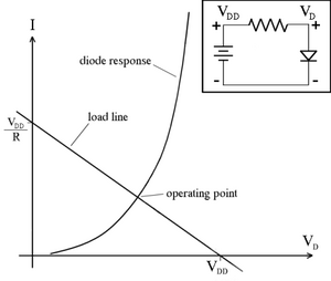
The example at right shows how a load line is used to determine the current and voltage in a simple diode circuit. The diode, a nonlinear device, is in series with a linear circuit consisting of a resistor, R and a voltage source, VDD. The characteristic curve (curved line), representing the current I through the diode for any given voltage across the diode VD, is an exponential curve. The load line (diagonal line), representing the relationship between current and voltage due to Kirchhoff's voltage law applied to the resistor and voltage source, is
Since the same current flows through each of the three elements in series, and the voltage produced by the voltage source and resistor is the voltage across the terminals of the diode, the operating point of the circuit will be at the intersection of the curve with the load line.
In a circuit with a three terminal device, such as a transistor, the current–voltage curve of the collector-emitter current depends on the base current. This is depicted on graphs by a series of (IC–VCE) curves at different base currents. A load line drawn on this graph shows how the base current will affect the operating point of the circuit.
Load lines for common configurations
Transistor load line

The load line diagram at right is for a resistive load in a common emitter circuit. The load line shows how the collector load resistor (RL) constrains the circuit voltage and current. The diagram also plots the transistor's collector current IC versus collector voltage VCE for different values of base current Ibase. The intersections of the load line with the transistor characteristic curves represent the circuit-constrained values of IC and VCE at different base currents.[2]
If the transistor could pass all the current available, with no voltage dropped across it, the collector current would be the supply voltage VCC over RL. This is the point where the load line crosses the vertical axis. Even at saturation, however, there will always be some voltage from collector to emitter.
Where the load line crosses the horizontal axis, the transistor current is minimum (approximately zero). The transistor is said to be cut off, passing only a very small leakage current, and so very nearly the entire supply voltage appears as VCE.
The operating point of the circuit in this configuration (labelled Q) is generally designed to be in the active region, approximately in the middle of the load line's active region for amplifier applications. Adjusting the base current so that the circuit is at this operating point with no signal applied is called biasing the transistor. Several techniques are used to stabilize the operating point against minor changes in temperature or transistor operating characteristics. When a signal is applied, the base current varies, and the collector-emitter voltage in turn varies, following the load line - the result is an amplifier stage with gain.
A load line is normally drawn on Ic-Vce characteristics curves for the transistor used in an amplifier circuit. The same technique is applied to other types of non-linear elements such as vacuum tubes or field effect transistors.
DC and AC load lines
Semiconductor circuits typically have both DC and AC currents in them, with a source of DC current to bias the nonlinear semiconductor to the correct operating point, and the AC signal superimposed on the DC. Load lines can be used separately for both DC and AC analysis. The DC load line is the load line of the DC equivalent circuit, defined by reducing the reactive components to zero (replacing capacitors by open circuits and inductors by short circuits). It is used to determine the correct DC operating point, often called the Q point.
Once a DC operating point is defined by the DC load line, an AC load line can be drawn through the Q point. The AC load line is a straight line with a slope equal to the AC impedance facing the nonlinear device, which is in general different from the DC resistance. The ratio of AC voltage to current in the device is defined by this line. Because the impedance of the reactive components will vary with frequency, the slope of the AC load line depends on the frequency of the applied signal. So there are many AC load lines, that vary from the DC load line (at low frequency) to a limiting AC load line, all having a common intersection at the DC operating point. This limiting load line, generally referred to as the AC load line, is the load line of the circuit at "infinite frequency", and can be found by replacing capacitors with short circuits, and inductors with open circuits.
References
- ↑ Adel Sedra, Kenneth Smith. Microelectronic Circuits, 5th ed.
- ↑ Maurice Yunik, Design of Modern Transistor Circuits, Prentice-Hall Inc., 1973 ISBN 0-13-201285-5 section 4.6 "Load Line Analysis" pp. 68-73
 |
