Engineering:Spreading resistance profiling
Spreading resistance profiling (SRP), also known as spreading resistance analysis (SRA), is a technique used to analyze resistivity versus depth in semiconductors. Semiconductor devices depend on the distribution of carriers (electrons or holes) within their structures to provide the desired performance. The carrier concentration (which can vary by up to ten orders of magnitude) can be inferred from the resistivity profile provided by SRP.
History
The fundamental relationship is usually attributed to James Clerk Maxwell (1831–1879). In 1962, Robert Mazur (US Patent 3,628,137) and Dickey[1] developed a practical 2-probe system using a pair of weighted osmium needles.
In 1970, Solid State Measurements was founded to manufacture spreading resistance profiling tools and in 1974, Solecon Labs was founded to provide spreading resistance profiling services. In 1980, Dickey developed a practical method of determining p- or n-type using the spreading resistance tool. Improvements have continued but have been challenged by the ever-shrinking dimensions of state-of-the-art digital devices. For shallow structures (<1 um deep), the data reduction is complex. Some of the contributors to the data reduction are Dickey,[2][3] Schumann and Gardner,[4] Choo et al.,[5] Berkowitz and Lux,[6] Evans and Donovan,[7] Peissens et al.,[8] Hu,[9] Albers,[10] and Casel and Jorke.[11]
Theory of operation
If a voltage is applied between two probe tips providing electrical contact to an infinite slab, the resistance encountered within the slab is , where:
- is the measured resistance in ohms,
- (rho) is the resistivity of the slab in ohm-cm, and
- is the radius of the contact area in cm.
Most of the resistance occurs very close to the electrical contact[12] allowing the local resistivity to be determined. The probes produce a negligible probe to silicon resistance (nearly ohmic contact) over the entire resistivity range for both p-type and n-type (rich in holes and rich in electrons respectively). Keeping the resistance of wiring and the spreading resistance within the probe tips to a minimum, the measured resistance is almost exclusively from for silicon samples at least thick. With the aid of calibration resistivity standards, can be determined at each probing by the probe pair.
Instrumentation
A bias of 5mV is applied across the probe tips. The measured resistance can range from 1-ohm to one billion ohms. A "log R" amplifier or electrometer is used to measure the resistance.
Mechanical

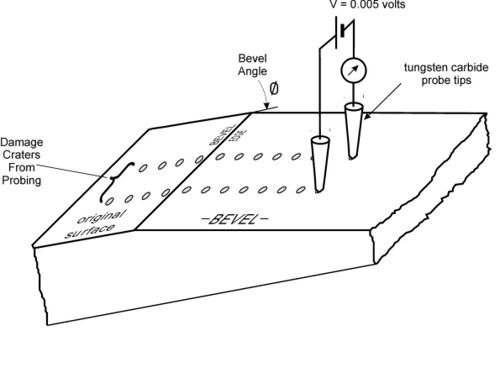
The modern SRP has two tungsten carbide probe tips placed about 20 um apart. Each tip is mounted on a kinematic bearing to minimize "scrubbing" (where the probes scratch along the surface). The probes are lowered very gently onto a beveled piece of silicon or germanium. Although the loading of the probe tips may be as little as 2 g., the pressure is in excess of one million pounds per sq inch (or ~ 10G pascals) causing a localized phase transformation in the silicon to "beta-tin" producing a nearly ohmic contact.[13] Between each measurement, the probes are raised and indexed a pre-determined distance down the bevel. Bevels are produced by mounting the sample on an angle block and grinding the bevel with typically a 0.1- or 0.05-micrometre diamond paste. Bevel angles, chosen to fit the depth of interest, can range from ~ 0.001 to 0.2 radians. Care must be used to produce a smooth, flat bevel with minimum rounding of the bevel edge. (See Figure 1.)
Detection limits
The instrument range is typically from one ohm to one billion ohms. This is adequate for the entire resistivity range in single-crystal silicon.
Calibration
Calibration standards have been produced by NIST. A set of 16 standards ranging from about 0.0006 ohm-cm to 200 ohm-cm have been produced for both n- and p-type and for both (100) and (111) crystal orientations. For high resistivity (above 200 ohm-cm and perhaps above 40,000 ohm-cm) the resistivity value must extrapolated from the calibration curve.
Applications
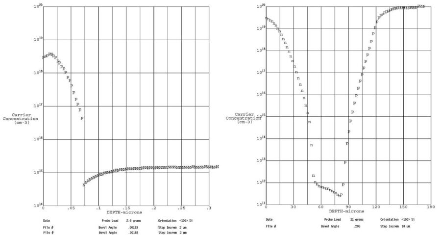
The tool is used primarily for determining doping structures in silicon semiconductors. Deep and shallow profiles are shown in Figure 2.

Alternative processes
Secondary ion mass spectrometry (SIMS) is also very useful for dopant profiling. SIMS can provide the atomic concentration over three decades or in some cases, four decades of dynamic range. SRP can determine the carrier concentration (electrically active dopant) in more than eight or nine decades of dynamic range. Often, the techniques are complementary although sometimes competitive. The equipment for SIMS tends to be considerably more expensive to manufacture and operate. While spreading resistance is limited to silicon, germanium and a few other semiconductors, SIMS can profile the atomic concentration of almost anything in anything. SIMS has greater spatial resolution useful for ultra-shallow profiles (< 0.1-micrometre) but SRP is more convenient for deeper structures.
References
- ↑ D. H. Dickey, The Electrochem. Soc., Electron. Div Ext. Abstr. 12, 151 (1963)
- ↑ D. H. Dickey and J. R. Ehrstein, NBS Special Publication 400-48, (1979)
- ↑ D. H. Dickey, ASTM Subcommittee F1.06 Meeting, Denver, June 1984
- ↑ P. A. Schumann and E. E. Gardner, J. Electrochem. Soc. 116, 87 (1969)
- ↑ S. C. Choo, M. S. Leong, and K.L. Hong, L. Li and L. S. Tan, Solid State Electronics, 21, 796 (1978)
- ↑ H. L. Berkowitz and R. A. Lux, J. Electrochem Soc. 128, 1137 (1981)
- ↑ R. A. Evans and R. P. Donovan, Solid St. Electron. 10, 155 (1967)
- ↑ R. Peissens, W. B. Vandervorst, and H. E. Maes, J. Electrochemical Soc. 130, 468 (1983).
- ↑ S. M. Hu, J. Appl. Phys. 53, 1499 (1982)
- ↑ J. H. Albers, Emerging Semiconductor Technology, ASTM ATP 960, D. C. Gupta and P. H. Langer, Eds., Am. Soc. for Testing and Materials (1986).
- ↑ A. Casel and H. Jorke, Appl. Phys. Lett., 50, 989 (1987)
- ↑ R. Holm, Electric Contacts, Almquist and Wiksels, Upsalla (1946)
- ↑ J. C. Jamieson, Crystal Structures at High Pressures of Metallic Modification of Silicon and Germanium, Science, 139 (1963)
Bibliography
R. G. Mazur and D. H. Dickey, A Spreading Resistance Technique for Resistivity Measurements on Silicon , J. Electrochem. Soc., 113, 255 (1966)
D. H. Dickey, History and Status of the Data Reduction Problem in SRA, Proceedings of the Third International Conference on Solid State and Integrated Circuit Technology, Ellwanger et al., Eds., Publishing House of Electronics Industry
M.W. Denhoff, An Accurate Calculation of Spreading Resistance, Journal of Physics D: Applied Physics, Volume 39, Number 9
External links
- Spreading_Resistance_Profiling
- Semilab
- Solecon Labs
- Tutorial on SRA process
- Additional technical notes
- An Accurate Calculation of Spreading Resistance
 |
