Engineering:UltraSPARC T2
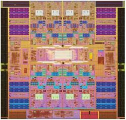
 UltraSPARC T2 Plus micrograph | |
| General Info | |
|---|---|
| Launched | 2007 |
| Designed by | Sun Microsystems |
| Common manufacturer(s) | |
| Performance | |
| Max. CPU clock rate | 1.2 GHz to 1.6 GHz |
| Architecture and classification | |
| Instruction set | SPARC V9 |
| Physical specifications | |
| Cores |
|
| Products, models, variants | |
| Core name(s) |
|
| History | |
| Predecessor | UltraSPARC T1 |
| Successor | SPARC T3 |
Sun Microsystems' UltraSPARC T2 microprocessor is a multithreading, multi-core CPU. It is a member of the SPARC family, and the successor to the UltraSPARC T1. The chip is sometimes referred to by its codename, Niagara 2. Sun started selling servers with the T2 processor in October 2007.
New features

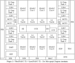
The T2 is a commodity derivative of the UltraSPARC series of microprocessors, targeting Internet workloads in computers, storage and networking devices. The processor, manufactured in 65 nm, is available with eight CPU cores, and each core is able to handle eight threads concurrently. Thus the processor is capable of processing up to 64 concurrent threads. Other new features include:[1]
- Speed bump for each thread, which increased the frequency from 1.2 GHz to 1.6 GHz
- One PCI Express port (x8 1.0) vs. the T1's JBus interface
- Two Sun Neptune 10 Gigabit Ethernet ports (embedded into the T2 processor) with packet classification and filtering
- L2 cache size increased to 4 MB (8-banks, 16-way associative) from 3 MB
- Improved thread scheduling and instruction prefetching to achieve higher single-threaded performance
- Two integer ALUs per core instead of one, each one being shared by a group of four threads
- One floating point unit per core, up from just one FPU for the entire chip
- Eight encryption engines, with each supporting DES, Triple DES, AES, RC4, SHA1, SHA256, MD5, RSA-2048, ECC, CRC-32
- Hardware random number generator
- Four dual-channel FBDIMM memory controllers
Core pipeline
There are 8 stages for integer operations, instead of 6 in the T1.
| Processor | Stages | |||||||
|---|---|---|---|---|---|---|---|---|
| T1's pipeline | Fetch | Thread Selection | Decode | Execute | Memory Access | Writeback | ||
| T2's pipeline | Fetch | Cache | Thread Selection | Decode | Execute | Memory Access | Bypass | Writeback |
Systems

The T2 processor can be found in the following products from Sun and Fujitsu Computer Systems:
- Sun/Fujitsu/Fujitsu Siemens SPARC Enterprise T5120 and T5220 servers
- Sun Blade T6320 Server Module
- Sun Netra CP3260 Blade
- Sun Netra T5220 Rackmount Server
Sun also licensed the T2 processor to Themis Computer, which introduced the first non-Sun T2-based servers in 2008:
- Themis T2BC Blade Server, which supports the entire family IBM BladeCenter chassis [2]
UltraSPARC T2 Plus

In April 2008, Sun released servers based on the UltraSPARC T2 Plus processor, an SMP capable version of UltraSPARC T2.[3]
Sun released the UltraSPARC T2 Plus processor with the following changes:
- Ability to be used in 2 or 4 processor configurations (first CoolThreads processor capable of multi-processor capability)
- Loss of on-chip embedded 10 Gigabit Ethernet controller
T2 Plus systems
UltraSPARC T2 Plus processors can be found in the following products from Sun and Fujitsu Computer Systems: Two-way SMP servers:
- Sun/Fujitsu/Fujitsu Siemens SPARC Enterprise T5140
- Sun/Fujitsu/Fujitsu Siemens SPARC Enterprise T5240
Four-way SMP server:
- Sun/Fujitsu/Fujitsu Siemens SPARC Enterprise T5440
Compute cluster
The High Performance Computing Virtual Laboratory in Canada built a compute cluster using 78 Sun SPARC Enterprise T5140 servers. With two 1.2 GHz T2 Plus chips in each T5140 server, the cluster has close to 10,000 compute threads, making it ideal for high-throughput workloads.[4]
Virtualization
Like the T1, the T2 supports the Hyper-Privileged execution mode. The SPARC Hypervisor runs in this mode and can partition a T2 system into 64 Logical Domains, and a two-way SMP T2 Plus system into 128 Logical Domains, each of which can run an independent operating system instance.
Performance improvement versus T1
The UltraSPARC T2 offers a variety of performance improvements over the former UltraSPARC T1 processor
- Integer throughput and throughput/watt (>2x improvement)
- Integer single-thread performance (>1.4x improvement)
- Better floating-point throughput (>10x improvement)
- Better floating-point single-thread performance (>5x improvement)
- Increased performance of cryptography through additional cyphers included in the embedded crypto cores
- Two world-record single-chip SPEC CPU results, based on tests that delivered 78.5 SPECint_rate2006 and 62.3 SPECfp_rate2006
Template:Application Tuning on the Coolthreads Platform
Other UltraSPARC T2 performance related tunings are documented on Oracle engineers' blogs.[5]
Power consumption
Peak power consumption can go as high as 123 watts, but the T2 typically consumes 95 watts during nominal system operation. This is up from 72 watts from the T1. Sun explains that this is due to a higher degree of system integration onto the chip.
Release history
On April 12, 2006, Sun announced the tape-out of the UltraSPARC T2.[6] Sun announced the T2's release on 7 August 2007, billing it as "the world's fastest microprocessor".[7]
On April 9, 2008, Sun announced the UltraSPARC T2 Plus.
Open design
On December 11, 2007, Sun made the UltraSPARC T2 processor design publicly available under the GNU General Public License via the OpenSPARC project. The release includes:
- Verilog RTL source code of the design
- Verification environment
- Diagnostics tests
- Open source tools, scripts and Sun internal tools needed to simulate the design
- ISA specification (UltraSPARC Architecture 2007)
- Solaris 10 OS simulation images
References
- ↑ "Niagara2: A Highly Threaded Server-on-a-Chip". http://www.opensparc.net/pubs/preszo/06/04-Sun-Golla.pdf.
- ↑ "T2BC Blade Servers". Themis Computer. 2008-06-02. http://www.themis.com/prod/t2bc.htm.
- ↑ "Sun Microsystems And Fujitsu Expand SPARC Enterprise Server Line With New UltraSPARC T2 Plus Processor-Based Systems". Sun Microsystems. 2008-04-09. http://www.sun.com/aboutsun/pr/2008-04/sunflash.20080409.1.xml.
- ↑ "Victoria Falls Cluster". HPCVL. 2008-06-10. http://www.hpcvl.org/hpc-environment/victoria-falls-cluster.
- ↑ "CMT Comes Of Age". Oracle. http://blogs.oracle.com/allanp/entry/cmt_comes_of_age.
- ↑ "Sun Microsystems Completes Design Tape-Out for Next-Generation, Breakthrough UltraSPARC T2 CoolThreads Processor". http://www.sun.com/smi/Press/sunflash/2006-04/sunflash.20060412.2.xml.
- ↑ "Announcement webcast". http://www.sun.com/featured-articles/2007-0807/feature/index.jsp.
External links
- OpenSPARC T2 and Specifications
- OpenSPARC Overview
- CMT Comes Of Age: Sun engineers give the inside scoop on the new UltraSPARC T2 systems
- CoolThreads Overview
- Niagara II: The Hydra Returns
 |
