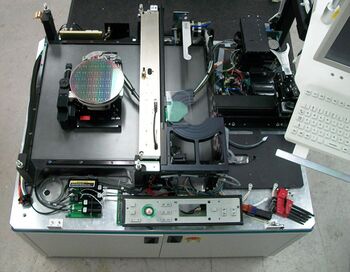
Engineering:Wafer testing
Wafer testing is a step performed during semiconductor device fabrication after BEOL process is finished. During this step, performed before a wafer is sent to die preparation, all individual integrated circuits that are present on the wafer are tested for functional defects by applying special test patterns to them. The wafer testing is performed by a piece of test equipment called a wafer prober. The process of wafer testing can be referred to in several ways: Wafer Final Test (WFT), Electronic Die Sort (EDS) and Circuit Probe (CP) are probably the most common.
Wafer prober

A wafer prober is a machine used for integrated circuits verification against designed functionality. It's either manual or automatic test equipment. For electrical testing a set of microscopic contacts or probes called a probe card are held in place whilst the wafer, vacuum-mounted on a wafer chuck, is moved into electrical contact. When a die (or array of dice) have been electrically tested the prober moves the wafer to the next die (or array) and the next test can start. The wafer prober is usually responsible for loading and unloading the wafers from their carrier (or cassette) and is equipped with automatic pattern recognition optics capable of aligning the wafer with sufficient accuracy to ensure accurate registration between the contact pads on the wafer and the tips of the probes.
For today's multi-die packages such as stacked chip-scale package (SCSP) or system in package (SiP) – the development of non-contact (RF) probes for identification of known tested die (KTD) and known good die (KGD) are critical to increasing overall system yield.
The wafer prober also exercises any test circuitry on the wafer scribe lines. Some companies get most of their information about device performance from these scribe line test structures.[1][2][3]
When all test patterns pass for a specific die, its position is remembered for later use during IC packaging. Sometimes a die has internal spare resources available for repairing (i.e. flash memory IC); if it does not pass some test patterns these spare resources can be used. If redundancy of failed die is not possible the die is considered faulty and is discarded. Non-passing circuits are typically marked with a small dot of ink in the middle of the die, or the information of passing/non-passing is stored in a file, named a wafermap. This map categorizes the passing and non-passing dies by making use of bins. A bin is then defined as a good or bad die. This wafermap is then sent to the die attachment process which then only picks up the passing circuits by selecting the bin number of good dies. The process where no ink dot is used to mark the bad dies is named substrate mapping. When ink dots are used, vision systems on subsequent die handling equipment can disqualify the die by recognizing the ink dot.
In some very specific cases, a die that passes some but not all test patterns can still be used as a product, typically with limited functionality. The most common example of this is a microprocessor for which only one part of the on-die cache memory is functional. In this case, the processor can sometimes still be sold as a lower cost part with a smaller amount of memory and thus lower performance. Additionally when bad dies have been identified, the die from the bad bin can be used by production personnel for assembly line setup.
The contents of all test patterns and the sequence by which they are applied to an integrated circuit are called the test program.
After IC packaging, a packaged chip will be tested again during the IC testing phase, usually with the same or very similar test patterns. For this reason, it may be thought that wafer testing is an unnecessary, redundant step. In reality this is not usually the case, since the removal of defective dies saves the considerable cost of packaging faulty devices. However, when the production yield is so high that wafer testing is more expensive than the packaging cost of defect devices, the wafer testing step can be skipped altogether and dies will undergo blind assembly.
See also
- Bond characterization
- Non-contact wafer testing
References
- ↑ "Startup enables IC variability characterization" by Richard Goering 2006
- ↑ "Testing LCD Source Driver IC with Built-on-Scribe-Line Test Circuitry" (abstract)
- ↑ Design for Manufacturability And Statistical Design: A Constructive Approach, by Michael Orshansky, Sani Nassif, Duane Boning 2007. ISBN 0-387-30928-4 ISBN 978-0-387-30928-6 [1] p. 84
Bibliography
- Fundamentals of Digital Semiconductor Testing (Version 4.0) by Guy A. Perry (Spiral-bound – Mar 1, 2003) ISBN 978-0965879705
- Principles of Semiconductor Network Testing (Test & Measurement) (Hardcover)by Amir Afshar, 1995 ISBN 978-0-7506-9472-8
- Power-Constrained Testing of VLSI Circuits. A Guide to the IEEE 1149.4 Test Standard (Frontiers in Electronic Testing) by Nicola Nicolici and Bashir M. Al-Hashimi (Kindle Edition – Feb 28, 2003) ISBN 978-0-306-48731-6
- Semiconductor Memories: Technology, Testing, and Reliability by Ashok K. Sharma (Hardcover – Sep 9, 2002) ISBN 978-0780310001
 |
