Organization:National Institute for Materials Science
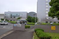
 Sengen site | |
Former names | NRIM, NIRIM |
|---|---|
| Type | Independent Administrative Institution |
| Established | 2001 |
| President | Kazuhito Hashimoto |
Administrative staff | 1500 |
| Location | Tsukuba , Ibaraki , Japan [ ⚑ ] : 36°04′26″N 140°07′15″E / 36.07388°N 140.12076°E |
| Campus | Sengen, Namiki, Sakura, Meguro |
| Website | www |
 | |
National Institute for Materials Science (物質・材料研究機構, Busshitsu-zairyō kenkyū kikō) is an Independent Administrative Institution and one of the largest scientific research centers in Japan .
History
The growth and development of today's scientific research center has passed through several phases in a number of locations:
In 1956, the National Research Institute for Metals (NRIM) was established in Meguro, Tokyo, Japan . In 1979, NRIM opened an office in Tsukuba. By 1995 the institute had moved most of its functions to that location. The Meguro campus continues to exist; it remains a part of the NRIM successor, the National Institute for Materials Science.
In 1966, the National Institute for Research in Inorganic Materials (NIRIM) was established in Toshima, Tokyo, Japan . NIRIM was moved to Tsukuba in 1972, in the very early stages of the Tsukuba Science City. This event was considered as the first transfer of a national research institute in Japan.
An independent administrative institute NIMS was established in Tsukuba by merging NRIM and NIRIM in 2001.
Campuses

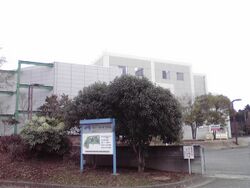
NIMS campuses are named Sengen, Namiki, Sakura, and Meguro. In addition, NIMS has a beamline station at the SPring-8 synchrotron located in Hyōgo Prefecture, Japan. While all campuses host scientific research units, most administration is in Sengen. In total, about 1500 researchers, engineers and administrative staff members are employed in all those campuses. Sengen, Namiki and Sakura branches are several kilometers apart in Tsukuba — a Science City within an hour from central Tokyo by Tsukuba Express train. A free shuttle bus facilitates transfer between the Tsukuba campuses.
Development
NIMS has developed as a dynamic organization; and new initiatives are launched virtually every month. Among the more noteworthy of these are:
- October 2001 Establishment of Biomaterials Center, Superconducting Materials Center, Computational Materials Science Center and Materials Information Technology Station
- April 2002 Establishment of Steel Research Center, Ecomaterials Center, High Magnetic Fields Center and Materials Analysis Station
- June 2002 Establishment of the Nanotechnology Researchers Network of Japan
- September 2003 Establishment of the International Center for Young Scientists (ICYS)
- April 2004 Establishment of Doctoral Program in Materials Science and Engineering of Graduate School of Pure and Applied Science, University of Tsukuba
- May 2004 Establishment of High Voltage Electron Microscopy Station
- April 2006 Start of the Second Mid-Term Program. This event coincided with significant reorganization of NIMS.
- October 2007 Establishment of the International Center for Materials Nanoarchitectonics (MANA)
Research
NIMS is dedicated to materials research with strong emphasis on the synthesis, characterization and applications of metals, semiconductors, superconductors, ceramics, and organic materials in their bulk and nanoscaled forms. The applications cover a wide range including electronics, optics, coatings, fuel cells, catalysts, and biotechnologies. As to characterization, techniques associated with electron microscopy, high-energy particle beams and high magnetic fields are particularly developed. Most research is experimental though at least one research center is devoted to theoretical modeling.
Selected achievements
NIMS has evolved into a recognized world leader in many scientific fields, including:
- Growth of single crystals of diamond[1] and boron nitride[2][3] by the high-pressure high-temperature technique.
- N-type doping of diamond thin films.[4]
- Beside synthesis of diamond and BN crystals and films, their optoelectronic applications have been demonstrated, such as deep-UV laser[3] and light-emitting diodes,[4][5]
- Growth and characterization of boron nitride nanotubes.[6]
- Superconducting[7] and organic[8] materials.
- Functional ceramics, such as superplastic ceramics,[9] etc.
- Catalyst nanoparticles.[10]
- Electron beam induced deposition – a technique of growing nanostructures and nanodevices using the beam of electron microscope.[11][12]
Besides, a number of novel devices and techniques have been proposed at NIMS:
- Atomic switch – a nano-scaled semiconducting device controlling movements of atoms.[13]
- The world smallest thermometer based on a single-wall carbon nanotube.[14]
- Giant electrostrain effect.[15]
- Warm spraying – an efficient technique of coating a substrate with a layer of metal, polymer or glass.[16]
Publications
- Science and Technology of Advanced Materials (STAM) – an international, peer-reviewed journal in materials science – has become an open access journal in 2008 through the NIMS sponsorship. The journal remains international, with its editors and referees located all over the world. Journal management is performed by the Scientific Information Office of NIMS, which has recently launched an initiative to drastically improve the prestige of STAM. The journal is printed by the Institute of Physics which maintains another STAM homepage.
- NIMS NOW International is a monthly newsletter of NIMS, which since July 2003 has been published exclusively for international readers. Monthly coverage includes NIMS latest research activities, management policy, progress in international collaborations, world-renowned guests, outstanding researchers and staff members, events, and other information, which reports current activities as well as key trends in materials science. NIMS NOW has more than 2400 subscribers in Japan and 73 countries worldwide. A printed version is available free of charge.
- Materials Science Outlook is a brochure intended for policy makers, research institute managers, and materials science researchers both domestic and overseas. This publication provides readers with detailed information to plan policies for their activities.
- NanotechJapan and Nanotech Magazine are regular publications of a MEXT-sponsored project. This collaborative project is hosted by NIMS and includes sharing scientific instrumentation between the 13 leading Japanese institutions.
Scientific cooperation
In September 2008, an innovative NIMS research unit, the International Center for Materials Nanoarchitectonics (MANA) embarked on a new program of scientific cooperation with the Yonsei University in Seoul, Korea. The exchange of researchers and research information between the two institutions is projected as a crucial factor in collaborative research on the development and evaluation of sustainable chemical technology and Nano-biofusion technology.[17]
Sister institutes
- Academia Sinica, Taiwan
- ETH Zurich, Switzerland
See also
- International Center for Materials Nanoarchitectonics (MANA)
- List of Independent Administrative Institutions (Japan)
- List of National Laboratories (Japan)
- Materials database
- Research Institutes in Tsukuba
- Versailles project on advanced materials and standards
References
- ↑ Akaishi, M.; Kanda, H.; Yamaoka, S. (1993-03-12). "Phosphorus: An Elemental Catalyst for Diamond Synthesis and Growth". Science (American Association for the Advancement of Science (AAAS)) 259 (5101): 1592–1593. doi:10.1126/science.259.5101.1592. ISSN 0036-8075.
- ↑ Kubota, Y.; Watanabe, K.; Tsuda, O.; Taniguchi, T. (2007-08-17). "Deep Ultraviolet Light-Emitting Hexagonal Boron Nitride Synthesized at Atmospheric Pressure". Science (American Association for the Advancement of Science (AAAS)) 317 (5840): 932–934. doi:10.1126/science.1144216. ISSN 0036-8075.
- ↑ 3.0 3.1 Watanabe, Kenji; Taniguchi, Takashi; Kanda, Hisao (2004-05-23). "Direct-bandgap properties and evidence for ultraviolet lasing of hexagonal boron nitride single crystal". Nature Materials (Springer Science and Business Media LLC) 3 (6): 404–409. doi:10.1038/nmat1134. ISSN 1476-1122.
- ↑ 4.0 4.1 Koizumi, S. (2001-06-08). "Ultraviolet Emission from a Diamond pn Junction". Science (American Association for the Advancement of Science (AAAS)) 292 (5523): 1899–1901. doi:10.1126/science.1060258. ISSN 0036-8075.
- ↑ Taniguchi, T.; Watanabe, K.; Koizumi, S.; Sakaguchi, I.; Sekiguchi, T.; Yamaoka, S. (2002-11-25). "Ultraviolet light emission from self-organized p–n domains in cubic boron nitride bulk single crystals grown under high pressure". Applied Physics Letters (AIP Publishing) 81 (22): 4145–4147. doi:10.1063/1.1524295. ISSN 0003-6951.
- ↑ Golberg, D.; Bando, Y.; Tang, C. C.; Zhi, C. Y. (2007-09-17). "Boron Nitride Nanotubes". Advanced Materials (Wiley) 19 (18): 2413–2432. doi:10.1002/adma.200700179. ISSN 0935-9648.
- ↑ Takada, Kazunori; Sakurai, Hiroya; Takayama-Muromachi, Eiji; Izumi, Fujio; Dilanian, Ruben A.; Sasaki, Takayoshi (2003). "Superconductivity in two-dimensional CoO2 layers". Nature (Springer Science and Business Media LLC) 422 (6927): 53–55. doi:10.1038/nature01450. ISSN 0028-0836.
- ↑ Peng, Xinsheng; Jin, Jian; Nakamura, Yoshimichi; Ohno, Takahisa; Ichinose, Izumi (2009-04-26). "Ultrafast permeation of water through protein-based membranes". Nature Nanotechnology (Springer Science and Business Media LLC) 4 (6): 353–357. doi:10.1038/nnano.2009.90. ISSN 1748-3387.
- ↑ Kim, B.-N.; Hiraga, K.; Morita, K.; Sakka, Y. (2001). "A high-strain-rate superplastic ceramic". Nature (Springer Science and Business Media LLC) 413 (6853): 288–291. doi:10.1038/35095025. ISSN 0028-0836.
- ↑ Zou, Zhigang; Ye, Jinhua; Sayama, Kazuhiro; Arakawa, Hironori (2001). "Direct splitting of water under visible light irradiation with an oxide semiconductor photocatalyst". Nature (Springer Science and Business Media LLC) 414 (6864): 625–627. doi:10.1038/414625a. ISSN 0028-0836.
- ↑ Furuya, Kazuo (2008). "Nanofabrication by advanced electron microscopy using intense and focused beam∗". Science and Technology of Advanced Materials (Informa UK Limited) 9 (1): 014110. doi:10.1088/1468-6996/9/1/014110. ISSN 1468-6996.
- ↑ Song, Minghui; Furuya, Kazuo (2008). "Fabrication and characterization of nanostructures on insulator substrates by electron-beam-induced deposition". Science and Technology of Advanced Materials (Informa UK Limited) 9 (2): 023002. doi:10.1088/1468-6996/9/2/023002. ISSN 1468-6996.
- ↑ Terabe, K.; Hasegawa, T.; Nakayama, T.; Aono, M. (2005). "Quantized conductance atomic switch". Nature (Springer Science and Business Media LLC) 433 (7021): 47–50. doi:10.1038/nature03190. ISSN 0028-0836.
- ↑ Gao, Yihua; Bando, Yoshio (2002). "Carbon nanothermometer containing gallium". Nature (Springer Science and Business Media LLC) 415 (6872): 599–599. doi:10.1038/415599a. ISSN 0028-0836.
- ↑ Ren, Xiaobing (2004-01-11). "Large electric-field-induced strain in ferroelectric crystals by point-defect-mediated reversible domain switching". Nature Materials (Springer Science and Business Media LLC) 3 (2): 91–94. doi:10.1038/nmat1051. ISSN 1476-1122.
- ↑ Kuroda, Seiji; Kawakita, Jin; Watanabe, Makoto; Katanoda, Hiroshi (2008). "Warm spraying—a novel coating process based on high-velocity impact of solid particles". Science and Technology of Advanced Materials (Informa UK Limited) 9 (3): 033002. doi:10.1088/1468-6996/9/3/033002. ISSN 1468-6996.
- ↑ "MANA signed a cooperation agreement with Yonsei University, Korea," News at NIMS. September 8, 2008.
External links
