Engineering:Electron microscope

An electron microscope is a microscope that uses a beam of electrons as a source of illumination. It uses electron optics that are analogous to the glass lenses of an optical light microscope to control the electron beam, for instance focusing it to produce magnified images or electron diffraction patterns. As the wavelength of an electron can be more than 100,000 times smaller than that of visible light, electron microscopes have a much higher resolution of about 0.1 nm, which compares to about 200 nm for light microscopes.[1] Electron microscope may refer to:
- Transmission electron microscope (TEM) where swift electrons go through a thin sample
- Scanning transmission electron microscope (STEM) which is similar to TEM with a scanned electron probe
- Scanning electron microscope (SEM) which is similar to STEM, but with thick samples
- Electron microprobe similar to a SEM, but more for chemical analysis
- Low-energy electron microscope (LEEM), used to image surfaces
- Photoemission electron microscope (PEEM) which is similar to LEEM using electrons emitted from surfaces by photons
Additional details can be found in the above links. This article contains some general information mainly about transmission and scanning electron microscopes.
History
Many developments laid the groundwork of the electron optics used in microscopes.[2] One significant step was the work of Hertz in 1883[3] who made a cathode-ray tube with electrostatic and magnetic deflection, demonstrating manipulation of the direction of an electron beam. Others were focusing of the electrons by an axial magnetic field by Emil Wiechert in 1899,[4] improved oxide-coated cathodes which produced more electrons by Arthur Wehnelt in 1905[5] and the development of the electromagnetic lens in 1926 by Hans Busch.[6] According to Dennis Gabor, the physicist Leó Szilárd tried in 1928 to convince him to build an electron microscope, for which Szilárd had filed a patent.[7]
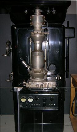
To this day the issue of who invented the transmission electron microscope is controversial.[8][9][10][11] In 1928, at the Technische Hochschule in Charlottenburg (now Technische Universität Berlin), Adolf Matthias (Professor of High Voltage Technology and Electrical Installations) appointed Max Knoll to lead a team of researchers to advance research on electron beams and cathode-ray oscilloscopes. The team consisted of several PhD students including Ernst Ruska. In 1931, Max Knoll and Ernst Ruska[12][13] successfully generated magnified images of mesh grids placed over an anode aperture. The device, a replicate of which is shown in the figure, used two magnetic lenses to achieve higher magnifications, the first electron microscope. (Max Knoll died in 1969, so did not receive a share of the 1986 Nobel prize for the invention of electron microscopes.)
Apparently independent of this effort was work at Siemens-Schuckert by Reinhold Rüdenberg. According to patent law (U.S. Patent No. 2058914[14] and 2070318,[15] both filed in 1932), he is the inventor of the electron microscope, but it is not clear when he had a working instrument. He stated in a very brief article in 1932[16] that Siemens had been working on this for some years before the patents were filed in 1932, claiming that his effort was parallel to the university development. He died in 1961, so similar to Max Knoll, was not eligible for a share of the 1986 Nobel prize.[17]
In the following year, 1933, Ruska and Knoll built the first electron microscope that exceeded the resolution of an optical (light) microscope.[18] Four years later, in 1937, Siemens financed the work of Ernst Ruska and Bodo von Borries, and employed Helmut Ruska, Ernst's brother, to develop applications for the microscope, especially with biological specimens.[18][19] Also in 1937, Manfred von Ardenne pioneered the scanning electron microscope.[20] Siemens produced the first commercial electron microscope in 1938.[21] The first North American electron microscopes were constructed in the 1930s, at the Washington State University by Anderson and Fitzsimmons [22] and at the University of Toronto by Eli Franklin Burton and students Cecil Hall, James Hillier, and Albert Prebus. Siemens produced a transmission electron microscope (TEM) in 1939.[23] Although current transmission electron microscopes are capable of two million times magnification, as scientific instruments they remain similar but with improved optics.
In the 1940s, high-resolution electron microscopes were developed, enabling greater magnification and resolution.[24] By 1965, Albert Crewe at the University of Chicago introduced the scanning transmission electron microscope using a field emission source,[25] enabling scanning microscopes at high resolution.[26] By the early 1980s improvements in mechanical stability as well as the use of higher accelerating voltages enabled imaging of materials at the atomic scale.[27][28] In the 1980s, the field emission gun became common for electron microscopes, improving the image quality due to the additional coherence and lower chromatic aberrations. The 2000s were marked by advancements in aberration-corrected electron microscopy, allowing for significant improvements in resolution and clarity of images.[29][30]
Types of electron microscopes
File:Transmission Electron Microscope operating principle.ogv
Transmission electron microscope (TEM)

The original form of the electron microscope, the transmission electron microscope (TEM), uses a high voltage electron beam to illuminate the specimen and create an image. An electron beam is produced by an electron gun, with the electrons typically having energies in the range 20 to 400 keV, focused by electromagnetic lenses, and transmitted through a thin specimen. When it emerges from the specimen, the electron beam carries information about the structure of the specimen that is then magnified by the lenses of the microscope. The spatial variation in this information (the "image") may be viewed by projecting the magnified electron image onto a detector. For example, the image may be viewed directly by an operator using a fluorescent viewing screen coated with a phosphor or scintillator material such as zinc sulfide. More commonly a high-resolution phosphor is coupled by means of a lens optical system or a fibre optic light-guide to the sensor of a digital camera. A different approach is to use a direct electron detector which has no scintillator, which addresses some of the limitations of scintillator-coupled cameras.[31]
For many years the resolution of TEMs was limited by aberrations of the electron optics, primarily the spherical aberration. In most recent instruments hardware correctors can reduce spherical aberration and other aberrations, improving the resolution in high-resolution transmission electron microscopy (HRTEM) to below 0.5 angstrom (50 picometres),[32] enabling magnifications of more than 50 million times.[33] The ability of HRTEM to determine the positions of atoms within materials is useful for many areas of research and development.[34]
Scanning electron microscope (SEM)
File:Scanning Electron Microscope.ogv
An SEM produces images by probing the specimen with a focused electron beam that is scanned across the specimen (raster scanning). When the electron beam interacts with the specimen, it loses energy and is scattered in different directions by a variety of mechanisms. These interactions lead to, among other events, emission of low-energy secondary electrons and high-energy backscattered electrons, light emission (cathodoluminescence) or X-ray emission. All of these signals carrying information about the specimen, such as the surface topography and composition. The image displayed when using an SEM shows the variation in the intensity of any of these signals as an image. In these each position in the image corresponding to a position of the beam on the specimen when the signal was generated.[35]: 1–15

SEMs are different from TEMs in that they use electrons with much lower energy, generally below 20 keV,[36] while TEMs generally use electrons with energies in the range of 80-300 keV.[37] Thus, the electron sources and optics of the two microscopes have different designs, and they are normally separate instruments.[38]
Scanning transmission electron microscope (STEM)
A STEM combines features of both a TEM and a SEM by rastering a focused incident probe across a specimen, but now mainly using the electrons which are transmitted through the sample. Many types of imaging are common to both TEM and STEM, but some such as annular dark-field imaging and other analytical techniques are much easier to perform with higher spatial resolutions in a STEM instrument. One drawback is that image data is acquired in serial rather than in parallel fashion.[35]: 75–138
Main operating modes
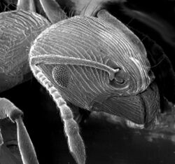
The most common methods of obtaining images in an electron microscope involve selecting different directions for the electrons that have been transmitted through a sample, and/or electrons of different energies. There are a very large number of methods of doing this, although not all are very common.
Secondary electrons
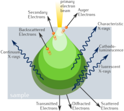
In a SEM the signals result from interactions of the electron beam with atoms within the sample. The most common mode is to use the secondary electrons (SE) to produce images. Secondary electrons have very low energies, on the order of 50 eV, which limits their mean free path in solid matter to a few nanometers below the sample surface.[39] The electrons are detected by an Everhart–Thornley detector,[40] which is a type of collector-scintillator-photomultiplier system. The signal from secondary electrons tends to be highly localized at the point of impact of the primary electron beam, making it possible to collect images of the sample surface with a resolution of better than 1 nm, and with specialized instruments at the atomic scale.[41]
The brightness of the signal depends on the number of secondary electrons reaching the detector. If the beam enters the sample perpendicular to the surface, then the electrons come out symmetrically about the axis of the beam. As the angle of incidence increases, the interaction volume from which they cone increases and the "escape" distance from one side of the beam decreases, resulting in more secondary electrons being emitted from the sample. Thus steep surfaces and edges tend to be brighter than flat surfaces, which results in images with a well-defined, three-dimensional appearance that is similar to a reflected light image.[39]
Backscattered electrons
Backscattered electrons (BSE) are those emitted back out from the specimen due to beam-specimen interactions where the electrons undergo elastic and inelastic scattering. They are conventionally defined as having energies from 50 eV up to the energy of the primary beam. Backscattered electrons can be used for both imaging and to form an electron backscatter diffraction (EBSD) image, the latter can be used to determine the crystallography of the specimen.[39]

Heavy elements (high atomic number) backscatter electrons more strongly than light elements (low atomic number), and thus appear brighter in the image, BSE images can therefore be used to detect areas with different chemical compositions.[39] To optimize the signal, dedicated backscattered electron detectors are positioned above the sample in a "doughnut" type arrangement, concentric with the electron beam, maximizing the solid angle of collection. BSE detectors are usually either scintillator or semiconductor types. When all parts of the detector are used to collect electrons symmetrically about the beam, atomic number contrast is produced. However, strong topographic contrast is produced by collecting back-scattered electrons from one side above the specimen using an asymmetrical, directional BSE detector; the resulting contrast appears as if there was illumination of the topography from that side. Semiconductor detectors can be made in radial segments that can be switched in or out to control the type of contrast produced and its directionality.[39]
Diffraction contrast imaging
Diffraction contrast uses the variation in either or both the direction of diffracted electrons or their amplitude as a function of position as the contrast mechanism. It is one of the simplest ways to image in a transmission electron microscope, and widely used.
The idea is to use an objective aperture below the sample and select only one or a range of different diffracted directions, then use these to form an image. When the aperture includes the incident beam direction the images are called bright field, since in the absence of any sample the field of view would be uniformly bright. When the aperture excludes the incident beam the images are called dark field, since similarly without a sample the image would be uniformly dark.[42][43] One variant of this is called weak-beam dark-field microscopy, and can be used to obtain high resolution images of defects such as dislocations.[44]
High resolution imaging

In high-resolution transmission electron microscopy (also sometimes called high-resolution electron microscopy) a number of different diffracted beams are allowed through the objective aperture. These interfere, leading to images which represent the atomic structure of the material. These can include the incident beam direction, or with scanning transmission electron microscopes they typically are for a range of diffracted beams excluding the incident beam.[28] Depending upon how thick the samples are and the aberrations of the microscope, these images can either be directly interpreted in terms of the positions of columns of atoms, or require a more careful analysis using calculations of the multiple scattering of the electrons[45] and the effect of the contrast transfer function of the microscope.[46]
There are many other imaging variants that can also to lead to atomic level information. Electron holography uses the interference of electrons which have been through the sample and a reference beam.[47] 4D STEM collects diffraction data at each point using a scanning instrument, then processes them to produce different types of images.[48]
X-ray microanalysis
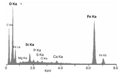
X-ray microanalysis is a method of obtaining local chemical information within electron microscopes of all types, although it is most commonly used in scanning instruments. When high energy electrons interact with atoms they can knock out electrons, particularly those in the inner shells and core electrons. These are then filled by valence electron, and the energy difference between the valence and core states can be converted into an x-ray which is detected by a spectrometer. The energies of these x-rays is somewhat specific to the atomic species, so local chemistry can be probed.[39]
EELS

Similar to X-ray microanalysis, the energies of electrons which have transmitted through a sample can be analyzed and yield information ranging from details of the local electronic structure to chemical information.[50]
Electron diffraction
Transmission electron microscopes can be used in electron diffraction mode where a map of the angles of the electrons leaving the sample is produced. The advantages of electron diffraction over X-ray crystallography are primarily in the size of the crystals. In X-ray crystallography, crystals are commonly visible by the naked eye and are generally in the hundreds of micrometers in length. In comparison, crystals for electron diffraction must be less than a few hundred nanometers in thickness, and have no lower boundary of size. Additionally, electron diffraction is done on a TEM, which can also be used to obtain other types of information, rather than requiring a separate instrument.[51][37]
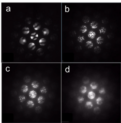
There are many variants on electron diffraction, depending upon exactly what type of illumination conditions are used. If a parallel beam is used with an aperture to limit the region exposed to the electrons then sharp diffraction features are normally observed, a technique called selected area electron diffraction. This is often the main technique used. Another common approach uses conical illumination and is called convergent beam electron diffraction (CBED). This is good for determining the symmetry of materials. A third is precession electron diffraction, where a parallel beam is spun around a large angle, producing a type of average diffraction pattern.[52] These often have less multiple scattering.[53]
Other electron microscope techniques
- Cathodoluminescence - analysing photons due to the electron beam
- Charge contrast imaging - using how charging varies with position to produce images
- CryoEM - using frozen samples, almost always biological samples
- EBSD - using the back-scattered electrons, typically in a SEM
- TKD - using the Kikuchi lines in diffraction patterns
- ECCI - using contrast due to electron channelling
- EBIC - measuring the current produced as a function of the position of a small beam
- Electron tomography - methods to produce 3D information by combining images
- FEM - technique to interrogate nanocrystalline materials
- Immune electron microscopy - the use of electron microscopy in immunology
- Geometric phase analysis - a method to analyze high-resolution images
- Serial block-face scanning electron microscopy - a way to produce 3D information from many images
- WDXS - higher precision detection of x-rays to analyze local chemistry
Aberration corrected instruments

Aberration-corrected transmission electron microscopy (AC-TEM) is the general term for electron microscopes where electro optical components are introduced to reduce the aberrations that would otherwise limit the resolution of the images. Historically electron microscopes had quite severe aberrations, and until about the start of the 21st century the resolution was limited, able to image the atomic structure of materials if the atoms were far enough apart.[54] Around the turn of the century the electron optical components were coupled with computer control of the lenses and their alignment, enabling correction of aberrations. The first demonstration of aberration correction in TEM mode was by Harald Rose and Maximilian Haider in 1998 using a hexapole corrector, and in STEM mode by Ondrej Krivanek and Niklas Dellby in 1999 using a quadrupole/octupole corrector.[55]
As of 2025 correction of geometric aberrations is standard in many commercial electron microscopes, and they are extensively used in many different areas of science.[56][57] Similar correctors have also been used at much lower energies for LEEM instruments.[58]
Sample preparation

Samples for electron microscopes mostly cannot be observed directly. The samples need to be prepared to stabilize the sample and enhance contrast. Preparation techniques differ vastly in respect to the sample and its specific qualities to be observed as well as the specific microscope used. Details can be found in the relevant main articles listed above.
Disadvantages

Electron microscopes are expensive to build and maintain. Microscopes designed to achieve high resolutions must be housed in stable buildings (sometimes underground) with special services such as magnetic field canceling systems and anti vibration mounts.[59]
The samples largely have to be viewed in vacuum, as the molecules that make up air would scatter the electrons. An exception is liquid-phase electron microscopy[60] using either a closed liquid cell or an environmental chamber, for example, in the environmental scanning electron microscope, which allows hydrated samples to be viewed in a low-pressure (up to 20 Torr or 2.7 kPa) wet environment. Various techniques for in situ electron microscopy of gaseous samples have also been developed.[61]

Samples of hydrated materials, including almost all biological specimens, have to be prepared in various ways to stabilize them, reduce their thickness (ultrathin sectioning) and increase their electron optical contrast (staining). These processes may result in artifacts, but these can usually be identified by comparing the results obtained by using radically different specimen preparation methods. Since the 1980s, analysis of cryofixed, vitrified specimens has also become increasingly used.[63][64][65]
Many samples suffer from radiation damage which can change internal structures. This can be due to either or both radiolytic processes or ballistic, for instance with collision cascades.[66] This can be a severe issue for biological samples.[67][68]
See also
- List of materials analysis methods
- Electron diffraction
- Electron energy loss spectroscopy (EELS)
- Energy filtered transmission electron microscopy (EFTEM)
- Environmental scanning electron microscope (ESEM)
- Immune electron microscopy
- In situ electron microscopy
- Low-energy electron microscopy
- Microscope image processing
- Microscopy
- Scanning confocal electron microscopy
- Scanning electron microscope (SEM)
- Thin section
- Transmission Electron Aberration-Corrected Microscope
- Volumetric Electron Microscopy
References
- ↑ "Electron microscope". https://www.britannica.com/technology/electron-microscope.
- ↑ "Historical Background of Electron Optics". Journal of Applied Physics 15 (10): 685–690. 1944. doi:10.1063/1.1707371. Bibcode: 1944JAP....15..685C.
- ↑ "Introduction to Heinrich Hertz's Miscellaneous Papers (1895) by Philipp Lenard". Heinrich Rudolf Hertz (1857-1894) : a collection of articles and addresses. Routledge. 2019. pp. 87–88. doi:10.4324/9780429198960-4. ISBN 978-0-429-19896-0.
- ↑ "Experimentelle Untersuchungen über die Geschwindigkeit und die magnetische Ablenkbarkeit der Kathodenstrahlen" (in de). Annalen der Physik und Chemie 305 (12): 739–766. 1899. doi:10.1002/andp.18993051203. Bibcode: 1899AnP...305..739W.
- ↑ "X. On the discharge of negative ions by glowing metallic oxides, and allied phenomena". The London, Edinburgh, and Dublin Philosophical Magazine and Journal of Science 10 (55): 80–90. 1905. doi:10.1080/14786440509463347.
- ↑ "Berechnung der Bahn von Kathodenstrahlen im axialsymmetrischen elektromagnetischen Felde" (in de). Annalen der Physik 386 (25): 974–993. 1926. doi:10.1002/andp.19263862507. Bibcode: 1926AnP...386..974B.
- ↑ Dannen, Gene (1998) Leo Szilard the Inventor: A Slideshow (1998, Budapest, conference talk). dannen.com
- ↑ "Origins and historical development of the electron microscope". British Journal of Applied Physics 13 (5): 197–207. 1962. doi:10.1088/0508-3443/13/5/303.
- ↑ "A Historical Investigation of the Debates on the Invention and Invention Rights of Electron Microscope". Proceedings of the 3rd International Conference on Contemporary Education, Social Sciences and Humanities (ICCESSH 2018). Advances in Social Science, Education and Humanities Research. Atlantis Press. 2018. pp. 1438–1441. doi:10.2991/iccessh-18.2018.313. ISBN 978-94-6252-528-3. https://www.atlantis-press.com/proceedings/iccessh-18/25898208.
- ↑ "Origin of the Electron Microscope". Science 142 (3589): 185–188. October 1963. doi:10.1126/science.142.3589.185. PMID 14057363. Bibcode: 1963Sci...142..185F.
- ↑ Origin and Background of the Invention of the Electron Microscope. Advances in Imaging and Electron Physics. 160. 2010. pp. 171–205. doi:10.1016/s1076-5670(10)60005-5. ISBN 978-0-12-381017-5..
- ↑ "Beitrag zur geometrischen Elektronenoptik. I". Annalen der Physik 404 (5): 607–640. 1932. doi:10.1002/andp.19324040506. Bibcode: 1932AnP...404..607K.
- ↑ "Das Elektronenmikroskop" (in de). Zeitschrift für Physik 78 (5–6): 318–339. 1932. doi:10.1007/BF01342199. Bibcode: 1932ZPhy...78..318K.
- ↑ "Apparatus for producing images of objects". https://image-ppubs.uspto.gov/dirsearch-public/print/downloadPdf/2058914.
- ↑ "Apparatus for producing images of objects". https://image-ppubs.uspto.gov/dirsearch-public/print/downloadPdf/2070318.
- ↑ Rüdenberg, R. (July 1932). "Elektronenmikroskop". Die Naturwissenschaften 20 (28): 522. doi:10.1007/BF01505383. Bibcode: 1932NW.....20..522R.
- ↑ "History of Electron Microscope". https://www.leo-em.co.uk/history-of-electron-microscope.html.
- ↑ 18.0 18.1 Ruska, Ernst (1986). "Ernst Ruska Autobiography". Nobel Foundation. http://nobelprize.org/nobel_prizes/physics/laureates/1986/ruska-autobio.html.
- ↑ "Helmut Ruska and the visualisation of viruses". Lancet 355 (9216): 1713–1717. May 2000. doi:10.1016/S0140-6736(00)02250-9. PMID 10905259.
- ↑ "Untersuchung von Metalloxyd-Rauchen mit dem Universal-Elektronenmikroskop" (in de). Zeitschrift für Elektrochemie und Angewandte Physikalische Chemie 46 (4): 270–277. 1940. doi:10.1002/bbpc.19400460406.
- ↑ History of electron microscopy, 1931–2000. Authors.library.caltech.edu (2002-12-10). Retrieved on 2017-04-29.
- ↑ "North America's first electron microscope". https://news.wsu.edu/2018/05/14/wsu-home-north-americas-first-electron-microscope/.
- ↑ "James Hillier". 2003-05-01. http://web.mit.edu/Invent/iow/hillier.html.
- ↑ The Beginnings of Electron Microscopy. Part 1. London San Diego, CA Cambridge, MA Oxford: Academic Press. 2021. ISBN 978-0-323-91507-6.
- ↑ Crewe, A. V.; Eggenberger, D. N.; Wall, J.; Welter, L. M. (1968-04-01). "Electron Gun Using a Field Emission Source". Review of Scientific Instruments 39 (4): 576–583. doi:10.1063/1.1683435. Bibcode: 1968RScI...39..576C.
- ↑ "Scanning electron microscopes: is high resolution possible?". Science 154 (3750): 729–738. November 1966. doi:10.1126/science.154.3750.729. PMID 17745977. Bibcode: 1966Sci...154..729C.
- ↑ Smith, David J.; Camps, R. A.; Freeman, L. A.; Hill, R.; Nixon, W. C.; Smith, K. C. A. (May 1983). "Recent improvements to the Cambridge University 600 kV High Resolution Electron Microscope". Journal of Microscopy 130 (2): 127–136. doi:10.1111/j.1365-2818.1983.tb04211.x.
- ↑ 28.0 28.1 Spence, John C. H. (2013). High-Resolution Electron Microscopy. doi:10.1093/acprof:oso/9780199668632.001.0001. ISBN 978-0-19-966863-2.
- ↑ Hawkes, P. W. (28 September 2009). "Aberration correction past and present". Philosophical Transactions of the Royal Society A: Mathematical, Physical and Engineering Sciences 367 (1903): 3637–3664. doi:10.1098/rsta.2009.0004. PMID 19687058. Bibcode: 2009RSPTA.367.3637H.
- ↑ Rose, H. H. (June 2009). "Historical aspects of aberration correction". Journal of Electron Microscopy 58 (3): 77–85. doi:10.1093/jmicro/dfp012. PMID 19254915.
- ↑ "A primer to single-particle cryo-electron microscopy". Cell 161 (3): 438–449. April 2015. doi:10.1016/j.cell.2015.03.050. PMID 25910204. Bibcode: 2015Cell..161..438C.
- ↑ "Atomic-resolution imaging with a sub-50-pm electron probe". Physical Review Letters 102 (9). March 2009. doi:10.1103/PhysRevLett.102.096101. PMID 19392535. Bibcode: 2009PhRvL.102i6101E. https://www.escholarship.org/uc/item/3cs0m4vr.
- ↑ "The Scale of Things". Office of Basic Energy Sciences, U.S. Department of Energy. 2006-05-26. http://www.sc.doe.gov/bes/scale_of_things.html.
- ↑ "Sub-Ångstrom Electron Microscopy for Sub-Ångstrom Nano-Metrology". Information Bridge: DOE Scientific and Technical Information – Sponsored by OSTI. 2004-01-18. http://www.osti.gov/bridge/servlets/purl/821768-E3YVgN/native/821768.pdf.
- ↑ 35.0 35.1 Kohl, Helmut; Reimer, Ludwig (2008). "Elements of a Transmission Electron Microscope". Transmission Electron Microscopy. Springer Series in Optical Sciences. 36. Springer. doi:10.1007/978-0-387-40093-8_4. ISBN 978-0-387-40093-8.
- ↑ "Choosing the Right Accelerating Voltage for SEM (An Introduction for Beginners)". Microscopy Today 18 (1): 48–52. January 2010. doi:10.1017/s1551929510991190.
- ↑ 37.0 37.1 "Electron Diffraction of 3D Molecular Crystals". Chemical Reviews 122 (17): 13883–13914. September 2022. doi:10.1021/acs.chemrev.1c00879. PMID 35970513.
- ↑ "Electron Microscopy | Thermo Fisher Scientific - US". 2022-04-07. https://www.thermofisher.com/us/en/home/electron-microscopy.html.
- ↑ 39.0 39.1 39.2 39.3 39.4 39.5 Goldstein, Joseph (2003-01-31) (in en). Scanning Electron Microscopy and X-Ray Microanalysis: Third Edition. Springer US. ISBN 978-0-306-47292-3. https://books.google.com/books?id=ruF9DQxCDLQC.
- ↑ Everhart, T. E.; Thornley, R. F. M. (1960). "Wide-band detector for micro-microampere low-energy electron currents". Journal of Scientific Instruments 37 (7): 246–248. doi:10.1088/0950-7671/37/7/307. Bibcode: 1960JScI...37..246E. http://authors.library.caltech.edu/12086/1/EVEjsi60.pdf.
- ↑ Ciston, J.; Brown, H. G.; D'Alfonso, A. J.; Koirala, P.; Ophus, C.; Lin, Y.; Suzuki, Y.; Inada, H. et al. (2015-06-17). "Surface determination through atomically resolved secondary-electron imaging" (in en). Nature Communications 6 (1). doi:10.1038/ncomms8358. ISSN 2041-1723. PMID 26082275. Bibcode: 2015NatCo...6.7358C.
- ↑ Hirsch, P. B.; Howie, A.; Nicholson, R. B.; Pashley, D. W.; Whelan, M. J. (1965). Electron microscopy of thin crystals. London: Butterworths. ISBN 0-408-18550-3. OCLC 2365578.
- ↑ Reimer, Ludwig (1997). "Transmission Electron Microscopy". Springer Series in Optical Sciences 36. doi:10.1007/978-3-662-14824-2. ISBN 978-3-662-14826-6. ISSN 0342-4111. Bibcode: 1997SSOS...36824.2R. https://doi.org/10.1007/978-3-662-14824-2.
- ↑ Cockayne, D. J. H.; Ray, I. L. F.; Whelan, M. J. (1969-12-01). "Investigations of dislocation strain fields using weak beams". The Philosophical Magazine 20 (168): 1265–1270. doi:10.1080/14786436908228210. ISSN 0031-8086. Bibcode: 1969PMag...20.1265C. https://www.tandfonline.com/doi/abs/10.1080/14786436908228210.
- ↑ Ishizuka, Kazuo (2004-02-01). "FFT Multislice Method—The Silver Anniversary". Microscopy and Microanalysis 10 (1): 34–40. doi:10.1017/S1431927604040292. ISSN 1431-9276. PMID 15306065. Bibcode: 2004MiMic..10...34I. https://academic.oup.com/mam/article-abstract/10/1/34/6912350?redirectedFrom=fulltext.
- ↑ Wade, R. H. (1992-10-01). "A brief look at imaging and contrast transfer". Ultramicroscopy 46 (1): 145–156. doi:10.1016/0304-3991(92)90011-8. ISSN 0304-3991. https://linkinghub.elsevier.com/retrieve/pii/0304399192900118.
- ↑ Cowley, J. M. (1992-06-01). "Twenty forms of electron holography". Ultramicroscopy 41 (4): 335–348. doi:10.1016/0304-3991(92)90213-4. ISSN 0304-3991. Bibcode: 1992Ultmi..41..335C. https://linkinghub.elsevier.com/retrieve/pii/0304399192902134.
- ↑ Ophus, Colin (2019-06-01). "Four-Dimensional Scanning Transmission Electron Microscopy (4D-STEM): From Scanning Nanodiffraction to Ptychography and Beyond". Microscopy and Microanalysis 25 (3): 563–582. doi:10.1017/S1431927619000497. ISSN 1431-9276. PMID 31084643. Bibcode: 2019MiMic..25..563O.
- ↑ Corbari, L (2008). "Iron oxide deposits associated with the ectosymbiotic bacteria in the hydrothermal vent shrimp Rimicaris exoculata". Biogeosciences 5 (5): 1295–1310. doi:10.5194/bg-5-1295-2008. Bibcode: 2008BGeo....5.1295C.
- ↑ Egerton, Ray F. (1986), "An Introduction to Electron Energy-Loss Spectroscopy", Electron Energy-Loss Spectroscopy in the Electron Microscope (Boston, MA: Springer US): pp. 1–25, doi:10.1007/978-1-4615-6887-2_1, ISBN 978-1-4615-6889-6, https://doi.org/10.1007/978-1-4615-6887-2_1, retrieved 2025-02-25
- ↑ Cowley, J. M. (1995). Diffraction physics. North Holland personal library (3rd ed.). Amsterdam: Elsevier. ISBN 978-0-444-82218-5.
- ↑ Vincent, R.; Midgley, P.A. (1994). "Double conical beam-rocking system for measurement of integrated electron diffraction intensities". Ultramicroscopy 53 (3): 271–82. doi:10.1016/0304-3991(94)90039-6.
- ↑ Own, C. S.: PhD thesis, System Design and Verification of the Precession Electron Diffraction Technique, Northwestern University, 2005,http://www.numis.northwestern.edu/Research/Current/precession.shtml
- ↑ Smith, David J (1997-12-01). "The realization of atomic resolution with the electron microscope". Reports on Progress in Physics 60 (12): 1513–1580. doi:10.1088/0034-4885/60/12/002. ISSN 0034-4885. Bibcode: 1997RPPh...60.1513S. https://doi.org/10.1088%2F0034-4885%2F60%2F12%2F002.
- ↑ Pennycook, S. J. (2012-12-01). "Seeing the atoms more clearly: STEM imaging from the Crewe era to today". Ultramicroscopy. Albert Victor Crewe Memorial Issue 123: 28–37. doi:10.1016/j.ultramic.2012.05.005. ISSN 0304-3991. PMID 22727567. https://www.sciencedirect.com/science/article/pii/S0304399112001076.
- ↑ Erni, Rolf (2015-03-23) (in en). Aberration-corrected Imaging In Transmission Electron Microscopy: An Introduction (2nd ed.). World Scientific Publishing Company. ISBN 978-1-78326-530-5. https://books.google.com/books?id=Gsw7DQAAQBAJ.
- ↑ Rose, Harald (2006-07-01). "Aberration correction in electron microscopy" (in en). International Journal of Materials Research 97 (7): 885–889. doi:10.1515/ijmr-2006-0143. ISSN 2195-8556. https://www.degruyterbrill.com:443/document/doi/10.1515/ijmr-2006-0143/html.
- ↑ Tromp, R.M.; Hannon, J.B.; Ellis, A.W.; Wan, W.; Berghaus, A.; Schaff, O. (June 2010). "A new aberration-corrected, energy-filtered LEEM/PEEM instrument. I. Principles and design" (in en). Ultramicroscopy 110 (7): 852–861. doi:10.1016/j.ultramic.2010.03.005. PMID 20395048. https://linkinghub.elsevier.com/retrieve/pii/S0304399110000835.
- ↑ "A Magnetic Field Canceling System Design for Diminishing Electromagnetic Interference to Avoid Environmental Hazard". International Journal of Environmental Research and Public Health 19 (6): 3664. March 2022. doi:10.3390/ijerph19063664. PMID 35329350.
- ↑ "Dynamic microscopy of nanoscale cluster growth at the solid-liquid interface". Nature Materials 2 (8): 532–536. August 2003. doi:10.1038/nmat944. PMID 12872162. Bibcode: 2003NatMa...2..532W.
- ↑ "Advances in atomic resolution in situ environmental transmission electron microscopy and 1A aberration corrected in situ electron microscopy". Microscopy Research and Technique 72 (3): 153–164. March 2009. doi:10.1002/jemt.20668. PMID 19140163.
- ↑ Demina, Tatiana A.; Oksanen, Hanna M. (2020-11-01). "Pleomorphic archaeal viruses: the family Pleolipoviridae is expanding by seven new species" (in en). Archives of Virology 165 (11): 2723–2731. doi:10.1007/s00705-020-04689-1. ISSN 1432-8798. PMID 32583077.
- ↑ "Cryo-electron microscopy of viruses". Nature 308 (5954): 32–36. 1984. doi:10.1038/308032a0. PMID 6322001. Bibcode: 1984Natur.308...32A. https://serval.unil.ch/resource/serval:BIB_BEC796503260.P001/REF.pdf.
- ↑ "Study of vitrified, unstained frozen tissue sections by cryoimmunoelectron microscopy". Journal of Cell Science 100 (1): 227–236. September 1991. doi:10.1242/jcs.100.1.227. PMID 1795028.
- ↑ "Vitrification of cryoelectron microscopy specimens revealed by high-speed photographic imaging". Journal of Microscopy 211 (Pt 1): 48–53. July 2003. doi:10.1046/j.1365-2818.2003.01193.x. PMID 12839550. http://infoscience.epfl.ch/record/109111.
- ↑ Egerton, R. F.; Li, P.; Malac, M. (2004-08-01). "Radiation damage in the TEM and SEM". Micron. International Wuhan Symposium on Advanced Electron Microscopy 35 (6): 399–409. doi:10.1016/j.micron.2004.02.003. ISSN 0968-4328. PMID 15120123. https://linkinghub.elsevier.com/retrieve/pii/S0968432804000381.
- ↑ Glaeser, Robert M. (1971-08-01). "Limitations to significant information in biological electron microscopy as a result of radiation damage". Journal of Ultrastructure Research 36 (3): 466–482. doi:10.1016/S0022-5320(71)80118-1. ISSN 0022-5320. PMID 5107051. https://linkinghub.elsevier.com/retrieve/pii/S0022532071801181.
- ↑ Baker, Lindsay A.; Rubinstein, John L. (2010-01-01), Jensen, Grant J., ed., "Chapter Fifteen - Radiation Damage in Electron Cryomicroscopy", Methods in Enzymology, Cryo-EM Part A Sample Preparation and Data Collection (Academic Press) 481: 371–388, doi:10.1016/s0076-6879(10)81015-8, PMID 20887865, https://linkinghub.elsevier.com/retrieve/pii/S0076687910810158, retrieved 2025-05-15
External links
| Library resources about Electron microscopy |
- An Introduction to Microscopy : resources for teachers and students
- Cell Centered Database – Electron microscopy data
 |
