Physics:Dielectric wireless receiver
Dielectric wireless receiver is a type of radiofrequency receiver front-end featuring a complete absence of electronic circuitry and metal interconnects. It offers immunity against damage from intense electromagnetic radiation, produced by EMP and HPM sources. This receiver is known as ADNERF (an acronym used to signify an All-Dielectric Non-Electronic Radio Front-End). ADNERF is a type of Electro-Magnetic Pulse Tolerant Microwave Receiver (EMPiRe).
Background
The continuing trend towards reduced feature size and voltage in integrated circuits renders modern electronics highly susceptible to damage caused by High Power Microwave (HPM) and other microwave based directed energy sources. These induce high voltage transient surges of thousands of volts which can punch through the gate insulator in the transistor and can destroy the circuit's metal interconnects. To immunize electronic systems against such threats, the “soft spots” (metal and transistor) in a conventional receiver front-end, must be eliminated.
Operation


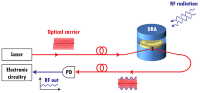
The basic concept of this photonic-assisted all-dielectric RF front-end technology is shown in Fig. 1. The Dielectric Resonator Antenna (DRA) in the front-end, functions as a concentrator of incoming electromagnetic field. When the electromagnetic (EM) field excites the resonance of DRA, a mode field pattern is built up inside the structure. The electro-optical (EO) resonator is placed at the location of the peak field magnitude (Fig. 2). The EO resonator converts the received EM signal to an intensity modulated optical signal which is then carried away from the antenna front-end via an optical fiber. At the remote location, the signal is converted back to an RF signal which is then amplified and processed using conventional techniques. This front-end design significantly increases the threshold for damage associated with high power microwave signals. The lack of metal interconnects eliminates the one source of failure. In addition, the charge isolation provided by the optical link protects the electronic circuitry. Good sensitivity can be achieved due to signal enhancement provided by the microwave resonance in the DRA and optical resonance in the EO resonator. The modulating E-field (ERF) applied to the resonator should not be uniform across the disk otherwise no modulation occurs. To prevent this from happening, the EO resonator is placed off center from the symmetrical axis of DRA as shown in Fig. 2. The location of the EO resonator is chosen to coincide with the peak EM field inside the DRA, which is identified using 3-D EM simulations. The field profile shown in Figure 2b does not include the presence of EO resonator. In practice the presence of the EO crystal will change the field distribution.
References
- Abrams, M. Dawn of the e-bomb. IEEE Spectrum 40, 24-30 (2003).[1]
- R. C. J. Hsu, A. Ayazi, B. Houshmand and B. Jalali, “All-Dielectric Photonic-Assisted Radio Front-End Technology,” Nature Photonics 1, 535–538 (2007).[2]
- A. Ayazi, C. J. Hsu, B. Houshmand, W. H. Steier, and B. Jalali, “All-dielectric photonics assisted wireless receiver,” Optics Express (2008).[3]
- DARPA's EMPiRe program. [4]
 |
