Physics:Silicon photomultiplier
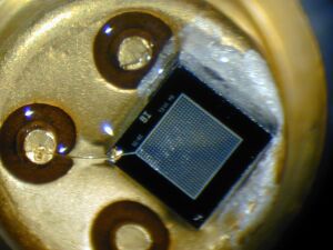
In solid-state electronics, silicon photomultipliers (SiPMs) are single-photon-sensitive devices based on single-photon avalanche diodes (SPADs) implemented on common silicon substrate.[1] The dimension of each single SPAD can vary from 10 to 100 micrometres, with a density of up to 10,000 per square millimeter. Every SPAD in a SiPM operates in Geiger mode and is coupled with the others by a metal or polysilicon quenching resistor. Although the device works in digital/switching mode, most SiPMs are analog devices because the microcells are read in parallel, making it possible to generate signals with a dynamic range from a single photon to 1000 photons for a device with just a square-millimeter area. More advanced readout schemes are used for lidar applications.[2] The supply voltage (Vb) depends on the APD technology used and typically varies between 20 V and 100 V, thus being from 15 to 75 times lower than the voltage required for traditional photomultiplier tube (PMT) operation.
Typical specifications for a SiPM:
- Photo detection efficiency (PDE) ranges from 20 to 50%, depending on device and wavelength, being similar to a traditional PMT
- Gain (G) is also similar to a PMT, being about 106
- G vs. Vb dependence is linear and does not follow a power law like in the case of PMTs
- Timing jitter is optimized to have a photon arrival time resolution of about 100-300 ps
- Signal decay time is inversely proportional to square root of photoelectrons number within an excitation event
- The signal parameters are practically independent of external magnetic fields, in contrast to vacuum PMTs
- Afterpulsing probability (3-30%), defined as probability of spurious second pulses after single photon arrival
- Dark count density is frequency of pulses in absence of illumination (105-106 pulses/s/mm2)
- Small dimensions and lower voltages permit extremely compact, light and robust mechanical design
SiPM for medical imaging are attractive candidates for the replacement of the conventional PMT in positron emission tomography (PET) and SPECT imaging, since they provide high gain with low voltage and fast response, they are very compact and compatible with magnetic resonance setups. Nevertheless, there are still several challenges, for example, SiPM requires optimization for larger matrices, signal amplification and digitization.
Comparison to vacuum tube photomultipliers
Advantages
Compared to conventional PMTs, the photoelectron gain in SiPMs is typically more deterministic, resulting in low or even negligible excess noise factor. As a result, the SNR (Signal-to-noise ratio) for a fixed number of detected photons can be higher than that from a PMT. Conversely, the stochastic gain of a PMT typically requires more detected photons to obtain the same SNR.
Mass production of silicon electronics by multiple vendors allows SiPMs to be made very cheaply relative to vacuum tubes.
Bias voltages are 10-100x times lower, simplifying electronics.
In the red to near-infrared, silicon enables much higher quantum efficiency than available PMT photocathode materials.
Dynamic range can be orders of magnitude larger than a PMT if large numbers of SPADs are arrayed together, enabling faster imaging rates or higher SNR without saturation.
Disadvantages
Dark current is typically much higher at a given temperature than a PMT. Thus, a SiPM may require subambient cooling while a PMT used in the same application may not, resulting in increased complexity and cost. Similarly, obtaining large active areas may be difficult due to higher dark counts per area than in PMTs.
The impulse response of a SiPM has a complex, multiexponential shape. Relative to a PMT, obtaining a symmetric pulse shape or uniform frequency response may require more complex analog filtering or pulse shaping electronics.
Comparison to avalanche photodiodes
Conventional avalanche photodiodes (APDs) also produce an amplified analog current in response to light absorption. However, in an APD, the total gain is much lower and the excess noise factor much higher. Conversely, quantum efficiency can be higher and dark noise lower.
See also
References
- ↑ Mascotto, Massimo (17 February 2011), Silicon Photomultiplier Technology at STMicroelectronics, https://indico.cern.ch/event/117424/contributions/1329247/attachments/56777/81753/STMicroelectronics_SIPM_CERN_2011-02-17.pdf, retrieved 25 July 2020
- ↑ A new generation, long distance ranging Time-of-Flight sensor based on ST’s FlightSense™ technology
de:Photomultiplier#Alternativen
 |


