Engineering:Wafer-level packaging
Wafer-level packaging (WLP) is a process where packaging components are attached to an integrated circuit (IC) before the wafer – on which the IC is fabricated – is diced. In WSP, the top and bottom layers of the packaging and the solder bumps are attached to the integrated circuits while they are still in the wafer. This process differs from a conventional process, in which the wafer is sliced into individual circuits (dice) before the packaging components are attached.
WLP is essentially a true chip-scale package (CSP) technology, since the resulting package is practically of the same size as the die. Wafer-level packaging allows integration of wafer fab, packaging, test, and burn-in at wafer level in order to streamline the manufacturing process undergone by a device from silicon start to customer shipment. There is no single industry-standard method of wafer-level packaging at present.
A major application area of WLPs are smartphones due to the size constraints. For example, the Apple iPhone 5 has at least eleven different WLPs, the Samsung Galaxy S3 has six WLPs and the HTC One X has seven. Functions provided WLPs in smartphones include sensors, power management, wireless, etc.[1] In fact, it has recently been rumored that the iPhone 7 will use fan-out wafer-level packaging technology in order to achieve a thinner and lighter model.[2][3][needs update]
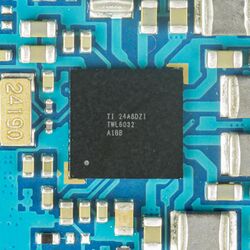
Wafer-level chip scale packaging (WL-CSP) is the smallest package currently available on the market and is produced by OSAT (Outsourced Semiconductor Assembly and Test) companies, such as Advanced Semiconductor Engineering (ASE).[4] A WL-CSP or WLCSP package is just a bare die with a redistribution layer (RDL, interposer or I/O pitch) to rearrange the pins or contacts on the die so that they can be big enough and have sufficient spacing so that they can be handled just like a ball grid array (BGA) package.[5]
There are two kinds of wafer level packaging: fan-in and fan-out. Fan-in WLCSP packages have an interposer that is the same size as that of the die, where as fan-out WLCSP packages have an interposer that is larger than the die, similar to conventional BGA packages, the difference being that the interposer is built directly atop the die, instead of the die being attached to it and reflowed using the flip chip method. This is also true in fan-in WLSCP packages.[6][7] In both cases, the die with its interposer may be covered in encapsulating material such as epoxy.
In February 2015, it was discovered that a WL-CSP chip in the Raspberry Pi 2 had issues with xenon flashes (or any other bright flashes of longwave light), inducing the photoelectric effect within the chip.[8] Thus, careful consideration concerning exposure to extremely bright light will need to be given with wafer-level packaging.
See also
References
- ↑ Korczynski, Ed (2014-05-05). "Wafer-level packaging of ICs for mobile systems of the future". Semiconductor Manufacturing & Design Community. http://semimd.com/blog/2014/05/05/wafer-level-packaging-of-ics-for-mobile-systems-of-the-future/.
- ↑ By Aaron Mamiit, Tech Times. “Apple Wants a Slimmer iPhone 7 and Will Reportedly Use Fan-Out Packaging Technology.” April 1, 2016. Retrieved April 8, 2016.
- ↑ By Yoni Heisler, BGR. “Report details new tech Apple is using to make the iPhone 7 thinner and lighter.” March 31, 2016. Retrieved April 14, 2016.
- ↑ By Mark LaPedus, Semiconductor Engineering. “Fan-Out Packaging Gains Steam.” November 23, 2015. Retrieved May 23, 2016.
- ↑ "Wafer Level Chip Scale Package (WLCSP)". https://www.nxp.com/docs/en/application-note/AN3846.pdf.
- ↑ "Stats ChipPAC - Wafer Level CSP (WLCSP) - a FIWLP Technology". http://www.statschippac.com/packaging/packaging/waferlevel/wlcsp.aspx.
- ↑ "WLCSP Overview, Market and Applications". November 11, 2018. https://anysilicon.com/wlcsp-overview-market-applications/.
- ↑ By Leon Spencer, ZDNet. “Raspberry Pi 2 power crashes when exposed to xenon flash.” February 9, 2015. Retrieved February 5, 2016.
Further reading
- Shichun Qu; Yong Liu (2014). Wafer-Level Chip-Scale Packaging: Analog and Power Semiconductor Applications. Springer. ISBN 978-1-4939-1556-9.
 |


