Physics:Quantum-confined Stark effect
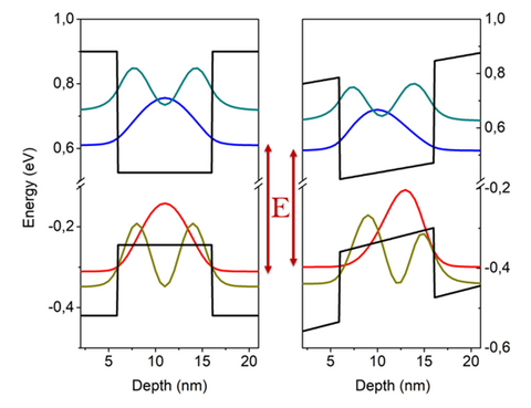
The quantum-confined Stark effect (QCSE) describes the effect of an external electric field upon the light absorption spectrum or emission spectrum of a quantum well (QW). In the absence of an external electric field, electrons and holes within the quantum well may only occupy states within a discrete set of energy subbands. Only a discrete set of frequencies of light may be absorbed or emitted by the system. When an external electric field is applied, the electron states shift to lower energies, while the hole states shift to higher energies. This reduces the permitted light absorption or emission frequencies. Additionally, the external electric field shifts electrons and holes to opposite sides of the well, decreasing the overlap integral, which in turn reduces the recombination efficiency (i.e. fluorescence quantum yield) of the system. [1] The spatial separation between the electrons and holes is limited by the presence of the potential barriers around the quantum well, meaning that excitons are able to exist in the system even under the influence of an electric field. The quantum-confined Stark effect is used in QCSE optical modulators, which allow optical communications signals to be switched on and off rapidly.[2]
Even if Quantum Objects (Wells, Dots or Discs, for instance) emit and absorb light generally with higher energies than the band gap of the material, the QCSE may shift the energy to values lower than the gap. This was evidenced recently in the study of quantum discs embedded in a nanowire.[3]
Theoretical description
The shift in absorption lines can be calculated by comparing the energy levels in unbiased and biased quantum wells. It is a simpler task to find the energy levels in the unbiased system, due to its symmetry. If the external electric field is small, it can be treated as a perturbation to the unbiased system and its approximate effect can be found using perturbation theory.
Unbiased system
The potential for a quantum well may be written as
- [math]\displaystyle{ V(z) = \begin{cases} 0; & |z| \lt L/2 \\ V_0; & \mbox{otherwise} \end{cases} }[/math],
where [math]\displaystyle{ L }[/math] is the width of the well and [math]\displaystyle{ V_0 }[/math] is the height of the potential barriers. The bound states in the well lie at a set of discrete energies, [math]\displaystyle{ E_n }[/math] and the associated wavefunctions can be written using the envelope function approximation as follows:
- [math]\displaystyle{ \psi(\mathbf{r})=\phi_{n}(z)\frac{1}{\sqrt{A}}e^{i(k_{x}\cdot{x}+k_{y}\cdot{y})}u(\mathbf{r}). }[/math]
In this expression, [math]\displaystyle{ A }[/math] is the cross-sectional area of the system, perpendicular to the quantization direction, [math]\displaystyle{ u(\mathbf{r}) }[/math] is a periodic Bloch function for the energy band edge in the bulk semiconductor and [math]\displaystyle{ \phi_n(z) }[/math] is a slowly varying envelope function for the system.

If the quantum well is very deep, it can be approximated by the particle in a box model, in which [math]\displaystyle{ V_0 \to \infty }[/math]. Under this simplified model, analytical expressions for the bound state wavefunctions exist, with the form
- [math]\displaystyle{ \phi_n(z) = \sqrt{\frac{2}{L}} \times \begin{cases} \cos \left(\frac{n\pi z}{L}\right) & n \, \text{odd} \\ \sin \left(\frac{n\pi z}{L}\right) & n \, \text{even} \end{cases}. }[/math]
The energies of the bound states are
- [math]\displaystyle{ E_n = \frac{\hbar^2n^2\pi^2}{2m^*L^2}, }[/math]
where [math]\displaystyle{ m^* }[/math] is the effective mass of an electron in a given semiconductor.
Biased system
Supposing the electric field is biased along the z direction,
- [math]\displaystyle{ \mathbf{F}=F\mathbf{z}, }[/math]
the perturbing Hamiltonian term is
- [math]\displaystyle{ H'=eFz. }[/math]
The first order correction to the energy levels is zero due to symmetry.
- [math]\displaystyle{ E_n^{(1)} = \langle n^{(0)} | eFz | n^{(0)} \rangle =0 }[/math].
The second order correction is, for instance n=1,
- [math]\displaystyle{ E_1^{(2)} = \sum_{k \ne 1} \frac{|\langle k^{(0)}|eFz|1^{(0)} \rangle|^2} {E_1^{(0)} - E_k^{(0)}} \approx \frac{|\langle 2^{(0)}|eFz|1^{(0)} \rangle|^2} {E_1^{(0)} - E_2^{(0)}} = -24\left(\frac{2}{3\pi}\right)^{6}\frac{e^{2}F^{2}m_e^{*}L^{4}}{\hbar^{2} } }[/math]
for electron, where the additional approximation of neglecting the perturbation terms due to the bound states with k even and > 2 has been introduced. By comparison, the perturbation terms from odd-k states are zero due to symmetry.
Similar calculations can be applied to holes by replacing the electron effective mass [math]\displaystyle{ m_e^* }[/math] with the hole effective mass [math]\displaystyle{ m_h^* }[/math]. Introducing the total effective mass [math]\displaystyle{ m_{tot}^* = m_e^* + m_h^* }[/math], the energy shift of the first optical transition induced by QCSE can be approximated to:
- [math]\displaystyle{ \Delta E \approx -24\left(\frac{2}{3\pi}\right)^{6}\frac{e^{2}F^{2}m_{tot}^{*}L^{4}}{\hbar^{2} }. }[/math][4]
- The downward shift in the confined energy level discussed in the above equation is referred to as the Franz-Keldysh effect.
The approximations made so far are quite crude, nonetheless the energy shift does show experimentally a square law dependence from the applied electric field,[5] as predicted.
Absorption coefficient
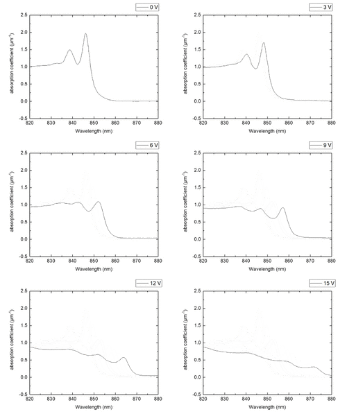
Additionally to the redshift towards lower energies of the optical transitions, the DC electric field also induces a decrease in magnitude of the absorption coefficient, as it decreases the overlapping integrals of relating valence and conduction band wave functions. Given the approximations made so far and the absence of any applied electric field along z, the overlapping integral for [math]\displaystyle{ n_{valence}=n_{conduction} }[/math] transitions will be:
- [math]\displaystyle{ \lang \phi_{c,n} | \phi_{v,n} \rang = 1 }[/math].
To calculate how this integral is modified by the quantum-confined Stark effect we once again employ time independent perturbation theory. The first order correction for the wave function is
- [math]\displaystyle{ \phi_n^' = \sum_{k \ne n} \frac{\lang \phi_n | H' | \phi_k \rang}{E_n - E_k} | \phi_k \rang }[/math].
Once again we look at the [math]\displaystyle{ n = 1 }[/math] energy level and consider only the perturbation from the level [math]\displaystyle{ n = 2 }[/math] (notice that the perturbation from [math]\displaystyle{ n = 3 }[/math] would be [math]\displaystyle{ = 0 }[/math] due to symmetry). We obtain
- [math]\displaystyle{ \phi_{c,1} = \phi_{c,1}^0 + \phi_{c,1}^' = \frac{1}{A} \left( \cos \left( \frac{\pi z}{L} \right) - \left( \frac{2}{3\pi} \right)^4 \frac{2 m_e^* e F L^3}{\hbar^2} \sin \left( \frac{\pi z}{L} \right) \right) }[/math]
- [math]\displaystyle{ \phi_{v,1} = \phi_{v,1}^0 + \phi_{v,1}^' = \frac{1}{A} \left( \cos \left( \frac{\pi z}{L} \right) + \left( \frac{2}{3\pi} \right)^4 \frac{2 m_h^* e F L^3}{\hbar^2} \sin \left( \frac{\pi z}{L} \right) \right) }[/math]
for the conduction and valence band respectively, where [math]\displaystyle{ A }[/math] has been introduced as a normalization constant. For any applied electric field [math]\displaystyle{ \vec{F} \cdot \hat{z} \ne 0 }[/math] we obtain
- [math]\displaystyle{ \lang \phi_{c,1} | \phi_{v,1} \rang \lt 1 }[/math].
Thus, according to Fermi's golden rule, which says that transition probability depends on the above overlapping integral, optical transition strength is weakened.
Excitons
The description of quantum-confined Stark effect given by second order perturbation theory is extremely simple and intuitive. However to correctly depict QCSE the role of excitons has to be taken into account. Excitons are quasiparticles consisting of a bound state of an electron-hole pair, whose binding energy in a bulk material can be modelled as that of an hydrogenic atom
- [math]\displaystyle{ E_{X,n} = \frac{\mu}{m_e\varepsilon_r^2}\frac{R_H}{n^2} }[/math]
where [math]\displaystyle{ R_H }[/math] is the Rydberg constant, [math]\displaystyle{ \mu }[/math] is the reduced mass of the electron-hole pair and [math]\displaystyle{ \varepsilon_r }[/math] is the relative electric permittivity. The exciton binding energy has to be included in the energy balance of photon absorption processes:
- [math]\displaystyle{ h\nu \gt E_g - E_{X} }[/math].
Exciton generation therefore redshift the optical band gap towards lower energies. If an electric field is applied to a bulk semiconductor, a further redshift in the absorption spectrum is observed due to Franz–Keldysh effect. Due to their opposite electric charges, the electron and the hole constituting the exciton will be pulled apart under the influence of the external electric field. If the field is strong enough
- [math]\displaystyle{ -e \vec{F} \cdot \vec{r_{X}} \gt |E_{X}| }[/math]
then excitons cease to exist in the bulk material. This somewhat limits the applicability of Franz-Keldysh for modulation purposes, as the redshift induced by the applied electric field is countered by shift towards higher energies due to the absence of exciton generations.
This problem does not exist in QCSE, as electrons and holes are confined in the quantum wells. As long as the quantum well depth is comparable to the excitonic Bohr radius, strong excitonic effects will be present no matter the magnitude of the applied electric field. Furthermore, quantum wells behave as two dimensional systems, which strongly enhance excitonic effects with respect to bulk material. In fact, solving the Schrödinger equation for a Coulomb potential in a two dimensional system yields an excitonic binding energy of
- [math]\displaystyle{ E_{X,n} = \frac{\mu}{m_e\varepsilon_r^2}\frac{R_H}{n^2-1/2} }[/math]
which is four times as high as the three dimensional case for the [math]\displaystyle{ 1s }[/math] solution.[6]
Optical modulation
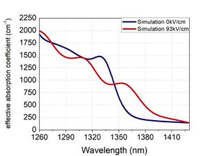
Quantum-confined Stark effect's most promising application lies in its ability to perform optical modulation in the near infrared spectral range, which is of great interest for silicon photonics and down-scaling of optical interconnects.[2][7] A QCSE based electro-absorption modulator consists of a PIN structure where the instrinsic region contains multiple quantum wells and acts as a waveguide for the carrier signal. An electric field can be induced perpendicularly to the quantum wells by applying an external, reverse bias to the PIN diode, causing QCSE. This mechanism can be employed to modulate wavelengths below the band gap of the unbiased system and within the reach of the QCSE induced redshift.
Although first demonstrated in GaAs/AlxGa1-xAs quantum wells,[1] QCSE started to generate interest after its demonstration in Ge/SiGe.[8] Differently from III/V semiconductors, Ge/SiGe quantum well stacks can be epitaxially grown on top of a silicon substrate, provided the presence of some buffer layer in between the two. This is a decisive advantage as it allows Ge/SiGe QCSE to be integrated with CMOS technology[9] and silicon photonics systems.
Germanium is an indirect gap semiconductor, with a bandgap of 0.66 eV. However it also has a relative minimum in the conduction band at the [math]\displaystyle{ \Gamma }[/math] point, with a direct bandgap of 0.8 eV, which corresponds to a wavelength of 1550 nm. QCSE in Ge/SiGe quantum wells can therefore be used to modulate light at 1.55 [math]\displaystyle{ \mu m }[/math],[9] which is crucial for silicon photonics applications as 1.55 [math]\displaystyle{ \mu m }[/math] is the optical fiber`s transparency window and the most extensively employed wavelength for telecommunications. By fine tuning material parameters such as quantum well depth, biaxial strain and silicon content in the well, it is also possible to tailor the optical band gap of the Ge/SiGe quantum well system to modulate at 1310 nm,[9][10] which also corresponds to a transparency window for optical fibers. Electro-optic modulation by QCSE using Ge/SiGe quantum wells has been demonstrated up to 23 GHz with energies per bit as low as 108 fJ.[11] and integrated in a waveguide configuration on a SiGe waveguide[12]
See also
Citations
- ↑ 1.0 1.1 Miller, D. (1984). "Band-Edge Electroabsorption in Quantum Well Structures: The Quantum-Confined Stark Effect". Phys. Rev. Lett. 53 (22): 2173–2176. doi:10.1103/PhysRevLett.53.2173. Bibcode: 1984PhRvL..53.2173M.
- ↑ 2.0 2.1 Miller, David A.B. (2009). "Device Requirements for Optical Interconnects to Silicon Chips". Proceedings of the IEEE 97 (7): 1166–1185. doi:10.1109/JPROC.2009.2014298.
- ↑ Zagonel, L. F. (2011). "Nanometer Scale Spectral Imaging of Quantum Emitters in Nanowires and Its Correlation to Their Atomically Resolved Structure". Nano Letters 11 (2): 568–573. doi:10.1021/nl103549t. PMID 21182283. Bibcode: 2011NanoL..11..568Z. http://www.stem.lps.u-psud.fr/research/correlating-structure-and-optical-emission-nanometric-quantum-emitters.
- ↑ Singh, Jasprit. Semiconductor Optolectronics: Physics and Technology. pp. Section 5.8: MODULATION OF EXCITONIC TRANSITIONS: QUANTUM CONFINED STARK EFFECT.
- ↑ Weiner, Joseph S.; Miller, David A. B.; Chemla, Daniel S. (30 March 1987). "Quadratic electro‐optic effect due to the quantum‐confined Stark effect in quantum wells". Applied Physics Letters 50 (13): 842–844. doi:10.1063/1.98008.
- ↑ Chuang, Shun Lien (2009). Physics of Photonics Devices, Chapter 3. Wiley. ISBN 978-0470293195.
- ↑ Miller, David A.B. (2017). "Attojoule Optoelectronics for Low-Energy Information Processing and Communications". Journal of Lightwave Technology 35 (3): 346–396. doi:10.1109/JLT.2017.2647779.
- ↑ Kuo, Yu-Hsuan; Lee, Yong Kyu; Ge, Yangsi; Ren, Shen; Roth, Jonathan E.; Kamins, Theodore I.; Miller, David A. B.; Harris, James S. (October 2005). "Strong quantum-confined Stark effect in germanium quantum-well structures on silicon". Nature 437 (7063): 1334–1336. doi:10.1038/nature04204. PMID 16251959.
- ↑ 9.0 9.1 9.2 Lever, L; Ikonić, Z; Valavanis, A; Cooper, J D; Kelsall, R W (November 2010). "Design of Ge–SiGe Quantum-Confined Stark Effect Electroabsorption Heterostructures for CMOS Compatible Photonics". Journal of Lightwave Technology. doi:10.1109/JLT.2010.2081345. http://eprints.whiterose.ac.uk/42668/4/IEEELever2010.pdf.
- ↑ Rouifed, Mohamed Said; Chaisakul, Papichaya; Marris-Morini, Delphine; Frigerio, Jacopo; Isella, Giovanni; Chrastina, Daniel; Edmond, Samson; Roux, Xavier Le et al. (18 September 2012). "Quantum-confined Stark effect at 13 μm in Ge/Si_035Ge_065 quantum-well structure". Optics Letters 37 (19): 3960–2. doi:10.1364/OL.37.003960. PMID 23027245.
- ↑ Chaisakul, Papichaya; Marris-Morini, Delphine; Rouifed, Mohamed-Saïd; Isella, Giovanni; Chrastina, Daniel; Frigerio, Jacopo; Le Roux, Xavier; Edmond, Samson et al. (26 January 2012). "23 GHz Ge/SiGe multiple quantum well electro-absorption modulator". Optics Express 20 (3): 3219–24. doi:10.1364/OE.20.003219. PMID 22330559.
- ↑ Chaisakul, Papichaya; Marris-Morini, Delphine; Frigerio, Jacopo; Chrastina, Daniel; Rouifed, Mohamed-Said; Cecchi, Stefano; Crozat, Paul; Isella, Giovanni et al. (11 May 2014). "Integrated germanium optical interconnects on silicon substrates". Nature Photonics 8 (6): 482–488. doi:10.1038/NPHOTON.2014.73.
General sources
- Mark Fox, Optical properties of solids, Oxford, New York, 2001.
- Hartmut Haug, Quantum Theory of the Optical and Electronic Properties of Semiconductors, World Scientific, 2004.
- https://web.archive.org/web/20100728030241/http://www.rle.mit.edu/sclaser/6.973%20lecture%20notes/Lecture%2013c.pdf
- Shun Lien Chuang, Physics of Photonics Devices, Wiley, 2009.
 |


