Chemistry:Low-energy plasma-enhanced chemical vapor deposition

Low-energy plasma-enhanced chemical vapor deposition (LEPECVD) is a plasma-enhanced chemical vapor deposition technique used for the epitaxial deposition of thin semiconductor (silicon, germanium and SiGe alloys) films. A remote low energy, high density DC argon plasma is employed to efficiently decompose the gas phase precursors while leaving the epitaxial layer undamaged, resulting in high quality epilayers and high deposition rates (up to 10 nm/s).
Working principle
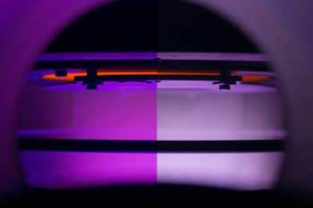
The substrate (typically a silicon wafer) is inserted in the reactor chamber, where it is heated by a graphite resistive heater from the backside. An argon plasma is introduced into the chamber to ionize the precursors' molecules, generating highly reactive radicals which result in the growth of an epilayer on the substrate. Moreover, the bombardment of Ar ions removes the hydrogen atoms adsorbed on the surface of the substrate while introducing no structural damage. The high reactivity of the radicals and the removal of hydrogen from the surface by ion bombardment prevent the typical problems of Si, Ge and SiGe alloys growth by thermal chemical vapor deposition (CVD), which are
- dependence of the growth rate from the substrate temperature, due to the thermal energy needed for precursors decomposition and hydrogen desorption from the substrate
- high temperatures (>1000 °C for silicon) required to get a significant growth rate, which is strongly limited by the aforementioned effects
- strong dependence of the deposition rate on the SiGe alloy composition, due to the large difference between the hydrogen desorption rate from Si and Ge surfaces.
Thanks to this effects the growth rate in a LEPECVD reactor depends only on the plasma parameters and the gas fluxes, and it is possible to obtain epitaxial deposition at much lower temperatures compared to a standard CVD tool.
LEPECVD reactor
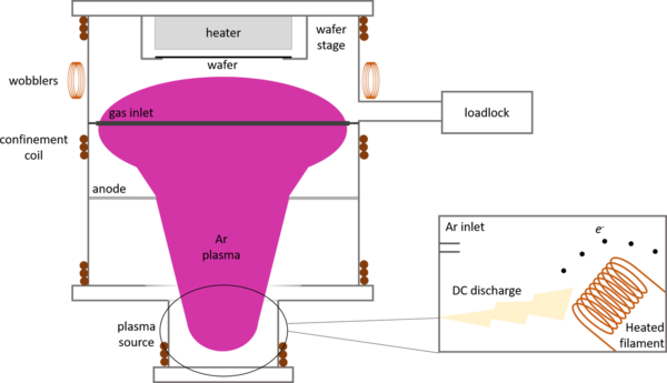
The LEPECVD reactor is divided in three main parts:
- a loadlock, to load the substrates into the chamber without breaking the vacuum
- the main chamber, which is kept in UHV at a base pressure of ~10[math]\displaystyle{ ^{-9} }[/math] mbar
- the plasma source, where the plasma is generated.
The substrate is placed at the top of the chamber, facing down toward the plasma source. Heating is provided from the back side by thermal radiation from a resistive graphite heater incapsulated between two boron nitride discs, which improve the temperature uniformity across the heater. Thermocouples are used to measure the temperature above the heater, which is then correlated to that of the substrate by a calibration done with an infrared pyrometer. Typical substrate temperatures for monocrystalline films are 400 °C to 760 °C, for germanium and silicon respectively.
The potential of the wafer stage can be controlled by an external power supply, influencing the amount and the energy of radicals impinging on the surface, and is typically kept at 10-15 V with respect to the chamber walls.
The process gases are introduced into the chamber through a gas dispersal ring placed below the wafer stage. The gases used in a LEPECVD reactor are silane (SiH
4) and germane (GeH
4) for silicon and germanium deposition respectively, together with diborane (B
2H
6) and phosphine (PH
3) for p- and n-type doping.
Plasma source
The plasma source is the most critical component of a LEPECVD reactor, as the low energy, high density, plasma is the key difference from a typical PECVD deposition system. The plasma is generated in a source which is attached to the bottom of the chamber. Argon is fed directly in the source, where tantalum filaments are heated to create an electron-rich environment by thermionic emission. The plasma is then ignited by a DC discharge from the heated filaments to the grounded walls of the source. Thanks to the high electron density in the source the voltage required to obtain a discharge is around 20-30V, resulting in an ion energy of about 10-20 eV, while the discharge current is of the order of several tens of amperes, giving a high ion density. The DC discharge current can be tuned to control the ion density, thus changing the growth rate: in particular at a larger discharge current the ion density is higher, therefore increasing the rate.
Plasma confinement
The plasma enters the growth chamber through an anode electrically connected to the grounded chamber walls, which is used to focus and stabilize the discharge and the plasma. Further focusing is provided by a magnetic field directed along the chamber's axis, provided by external copper coils wrapped around the chamber. The current flowing through the coils (i.e. the intensity of the magnetic field) can be controlled to change the ion density at the substrate's surface, thus changing the growth rate. Additional coils ("wobblers") are placed around the chamber, with their axis perpendicular to the magnetic field, to continuously sweep the plasma over the substrate, improving the homogeneity of the deposited film.
Applications
Thanks to the possibility of changing the growth rate (through the plasma density or gas fluxes) independently from the substrate temperature, both thin films with sharp interfaces and a precision down to the nanometer scale at rates as low as 0.4 nm/s, as well as thick layers (up to 10 um or more) at rates as high as 10 nm/s, can be grown using the same reactor and in the same deposition process. This has been exploited to grow low-loss composition-graded waveguides for NIR[1] and MIR[2] and integrated nanostructures (i.e. quantum well stacks) for NIR optical amplitude modulation.[1] The capability of LEPECVD to grow both very sharp quantum wells on thick buffers in the same deposition step has also been employed to realize high mobility strained Ge channels.[3]
Another promising application of the LEPECVD technique is the possibility of growing high aspect ratio, self-assembled silicon and germanium microcrystals on deeply patterned Si substrates.[4] This solves many problems related to heteroepitaxy (i.e. thermal expansion coefficient and crystal lattice mismatch), leading to very high crystal quality, and is possible thanks to the high rates and low temperatures found in a LEPECVD reactor.[5]
See also
References
- ↑ 1.0 1.1 Vivien, Laurent; Isella, Giovanni; Crozat, Paul; Cecchi, Stefano; Rouifed, Mohamed-Said; Chrastina, Daniel; Frigerio, Jacopo; Marris-Morini, Delphine et al. (June 2014). "Integrated germanium optical interconnects on silicon substrates" (in en). Nature Photonics 8 (6): 482–488. doi:10.1038/nphoton.2014.73. ISSN 1749-4893.
- ↑ Ramirez, J. M.; Liu, Q.; Vakarin, V.; Frigerio, J.; Ballabio, A.; Le Roux, X.; Bouville, D.; Vivien, L. et al. (9 January 2018). "Graded SiGe waveguides with broadband low-loss propagation in the mid infrared". Optics Express 26 (2): 870–877. doi:10.1364/OE.26.000870. PMID 29401966. https://zenodo.org/record/3504295.
- ↑ von Känel, H.; Chrastina, D.; Rössner, B.; Isella, G.; Hague, J.P.; Bollani, M. (October 2004). "High mobility SiGe heterostructures fabricated by low-energy plasma-enhanced chemical vapor deposition". Microelectronic Engineering 76 (1–4): 279–284. doi:10.1016/j.mee.2004.07.029.
- ↑ Falub, C. V.; von Kanel, H.; Isa, F.; Bergamaschini, R.; Marzegalli, A.; Chrastina, D.; Isella, G.; Muller, E. et al. (15 March 2012). "Scaling Hetero-Epitaxy from Layers to Three-Dimensional Crystals". Science 335 (6074): 1330–1334. doi:10.1126/science.1217666. PMID 22422978.
- ↑ Bergamaschini, R.; Isa, F.; Falub, C.V.; Niedermann, P.; Müller, E.; Isella, G.; von Känel, H.; Miglio, L. (November 2013). "Self-aligned Ge and SiGe three-dimensional epitaxy on dense Si pillar arrays". Surface Science Reports 68 (3–4): 390–417. doi:10.1016/j.surfrep.2013.10.002.
External links
- LEPECVD page on the website of L-NESS laboratory of Politecnico di Milano, in Como, Italy.


