Chemistry:Plasma-enhanced chemical vapor deposition
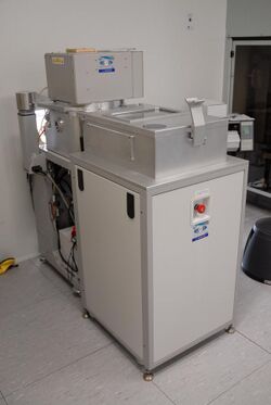
Plasma-enhanced chemical vapor deposition (PECVD) is a chemical vapor deposition process used to deposit thin films from a gas state (vapor) to a solid state on a substrate. Chemical reactions are involved in the process, which occur after creation of a plasma of the reacting gases. The plasma is generally created by radio frequency (RF) (alternating current (AC)) frequency or direct current (DC) discharge between two electrodes, the space between which is filled with the reacting gases.
Discharges for processes
A plasma is any gas in which a significant percentage of the atoms or molecules are ionized. Fractional ionization in plasmas used for deposition and related materials processing varies from about 10−4 in typical capacitive discharges to as high as 5–10% in high-density inductive plasmas. Processing plasmas are typically operated at pressures of a few millitorrs to a few torr, although arc discharges and inductive plasmas can be ignited at atmospheric pressure. Plasmas with low fractional ionization are of great interest for materials processing because electrons are so light, compared to atoms and molecules, that energy exchange between the electrons and neutral gas is very inefficient. Therefore, the electrons can be maintained at very high equivalent temperatures – tens of thousands of kelvins, equivalent to several electronvolts average energy—while the neutral atoms remain at the ambient temperature. These energetic electrons can induce many processes that would otherwise be very improbable at low temperatures, such as dissociation of precursor molecules and the creation of large quantities of free radicals.
The second benefit of deposition within a discharge arises from the fact that electrons are more mobile than ions. As a consequence, the plasma is normally more positive than any object it is in contact with, as otherwise, a large flux of electrons would flow from the plasma to the object. The difference in voltage between the plasma and the objects in its contacts normally occurs across a thin sheath region. Ionized atoms or molecules that diffuse to the edge of the sheath region feel an electrostatic force and are accelerated towards the neighboring surface. Thus, all surfaces exposed to the plasma receive energetic ion bombardment. The potential across the sheath surrounding an electrically isolated object (the floating potential) is typically only 10–20 V, but much higher sheath potentials are achievable by adjustments in reactor geometry and configuration. Thus, films can be exposed to energetic ion bombardment during deposition. This bombardment can lead to increases in the density of the film, and help remove contaminants, improving the film's electrical and mechanical properties. When a high-density plasma is used, the ion density can be high enough that significant sputtering of the deposited film occurs; this sputtering can be employed to help planarize the film and fill trenches or holes.
Reactor types
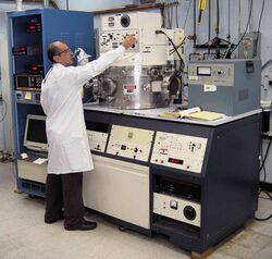
A simple DC discharge can be readily created at a few torr between two conductive electrodes, and may be suitable for deposition of conductive materials. However, insulating films will quickly extinguish this discharge as they are deposited. It is more common to excite a capacitive discharge by applying an AC or RF signal between an electrode and the conductive walls of a reactor chamber, or between two cylindrical conductive electrodes facing one another. The latter configuration is known as a parallel plate reactor. Frequencies of a few tens of Hz to a few thousand Hz will produce time-varying plasmas that are repeatedly initiated and extinguished; frequencies of tens of kilohertz to tens of megahertz result in reasonably time-independent discharges.
Excitation frequencies in the low-frequency (LF) range, usually around 100 kHz, require several hundred volts to sustain the discharge. These large voltages lead to high-energy ion bombardment of surfaces. High-frequency plasmas are often excited at the standard 13.56 MHz frequency widely available for industrial use; at high frequencies, the displacement current from sheath movement and scattering from the sheath assist in ionization, and thus lower voltages are sufficient to achieve higher plasma densities. Thus one can adjust the chemistry and ion bombardment in the deposition by changing the frequency of excitation, or by using a mixture of low- and high-frequency signals in a dual-frequency reactor. Excitation power of tens to hundreds of watts is typical for an electrode with a diameter of 200 to 300 mm.
Capacitive plasmas are usually very lightly ionized, resulting in limited dissociation of precursors and low deposition rates. Much denser plasmas can be created using inductive discharges, in which an inductive coil excited with a high-frequency signal induces an electric field within the discharge, accelerating electrons in the plasma itself rather than just at the sheath edge. Electron cyclotron resonance reactors and helicon wave antennas have also been used to create high-density discharges. Excitation powers of 10 kW or more are often used in modern reactors.
High density plasmas can also be generated by a DC discharge in an electron-rich environment, obtained by thermionic emission from heated filaments. The voltages required by the arc discharge are of the order of a few tens of volts, resulting in low energy ions. The high density, low energy plasma is exploited for the epitaxial deposition at high rates in Low-Energy Plasma-Enhanced chemical vapor deposition reactors.
Origins
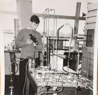
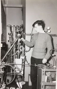
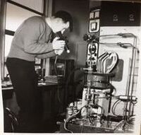
Working at Standard Telecommunication Laboratories (STL), Harlow, Essex, R C G Swann discovered that RF discharge promoted the deposition of silicon compounds onto the quartz glass vessel wall.[1] Several internal STL publications were followed in 1964 by French,[2] British[3] and US[4] patent applications. An article was published in the August 1965 volume of Solid State Electronics.[5]
Film examples and applications
Plasma deposition is often used in semiconductor manufacturing to deposit films conformally (covering sidewalls) and onto wafers containing metal layers or other temperature-sensitive structures. PECVD also yields some of the fastest deposition rates while maintaining film quality (such as roughness, defects/voids), as compared with sputter deposition and thermal/electron-beam evaporation, often at the expense of uniformity.
Silicon dioxide deposition
Silicon dioxide can be deposited using a combination of silicon precursor gasses like dichlorosilane or silane and oxygen precursors, such as oxygen and nitrous oxide, typically at pressures from a few millitorr to a few torr. Plasma-deposited silicon nitride, formed from silane and ammonia or nitrogen, is also widely used, although it is important to note that it is not possible to deposit a pure nitride in this fashion. Plasma nitrides always contain a large amount of hydrogen, which can be bonded to silicon (Si-H) or nitrogen (Si-NH);[6] this hydrogen has an important influence on IR and UV absorption,[7] stability, mechanical stress, and electrical conductivity.[8] This is often used as a surface and bulk passivating layer for commercial multicrystalline silicon photovoltaic cells.[9]
Silicon dioxide can also be deposited from a tetraethylorthosilicate (TEOS) silicon precursor in an oxygen or oxygen-argon plasma. These films can be contaminated with significant carbon and hydrogen as silanol, and can be unstable in air[citation needed]. Pressures of a few torr and small electrode spacings, and/or dual frequency deposition, are helpful to achieve high deposition rates with good film stability.
High-density plasma deposition of silicon dioxide from silane and oxygen/argon has been widely used to create a nearly hydrogen-free film with good conformality over complex surfaces, the latter resulting from intense ion bombardment and consequent sputtering of the deposited molecules from vertical onto horizontal surfaces[citation needed].
See also
- Low-Energy Plasma-Enhanced chemical vapor deposition
References
- ↑ "First-Hand:The Birth of Glow Discharge Chemistry (aka PECVD) - Engineering and Technology History Wiki" (in en). 17 March 2015. http://ethw.org/First-Hand:The_Birth_of_Glow_Discharge_Chemistry_(aka_PECVD).
- ↑ Sterling and Swann. "Perfectionnements aux méthodes de formation de couches" (in en). https://bases-brevets.inpi.fr/en/document-en/FR1442502/publications.html.
- ↑ Sterling and Swann, Improvements in or relating to a method of forming a layer of an inorganic compound, https://patents.google.com/patent/GB1104935A/en
- ↑ Sterling and Swann, Method of forming silicon oxide coatings in an electric discharge, https://patents.google.com/patent/US3655438A/en
- ↑ Sterling, H.F; Swann, R.C.G (1965-08-01). "Chemical vapour deposition promoted by r.f. discharge" (in en). Solid-State Electronics 8 (8): 653–654. doi:10.1016/0038-1101(65)90033-X. ISSN 0038-1101. Bibcode: 1965SSEle...8..653S.
- ↑ Ay and Aydinli. Comparative investigation of hydrogen bonding in silicon based PECVD grown dielectrics for optical waveguides. Optical Materials (2004) vol. 26 (1) pp. 33-46
- ↑ Albers et al. Reduction of hydrogen induced losses in PECVD-SiOxNy optical waveguides in the near infrared. Lasers and Electro-Optics Society Annual Meeting, 1995. 8th Annual Meeting Conference Proceedings, Volume 1., IEEE (1995) vol. 2 pp. 88-89 vol. 2
- ↑ G. Tellez et al., INFRARED CHARACTERIZATION OF SiN FILMS ON Si FOR HIGH SPEED ELECTRONICS APPLICATIONS. MASTER OF SCIENCE IN APPLIED PHYSICS, Naval Postgraduate School, Monterey, California, USA (2004)
- ↑ El amrani, A.; Menous, I.; Mahiou, L.; Tadjine, R.; Touati, A.; Lefgoum, A. (2008-10-01). "Silicon nitride film for solar cells". Renewable Energy 33 (10): 2289–2293. doi:10.1016/j.renene.2007.12.015.
