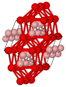
Chemistry:Nickel monosilicide

| |
| Identifiers | |
|---|---|
3D model (JSmol)
|
|
PubChem CID
|
|
| |
| |
| Properties | |
| NiSi | |
| Molar mass | 86.778 g/mol |
| Melting point | 1,000 °C; 1,832 °F; 1,273 K[2] |
| -0.3×10⁻⁶ emu/g[1] | |
| Structure[3] | |
| Orthorhombic, oP8 | |
| Pnma, No. 62 | |
a = 0.519 nm, b = 0.333 nm, c = 0.5628 nm
| |
Formula units (Z)
|
4 |
Except where otherwise noted, data are given for materials in their standard state (at 25 °C [77 °F], 100 kPa). | |
| Infobox references | |
Nickel monosilicide is an intermetallic compound formed out of nickel and silicon. Like other nickel silicides, NiSi is of importance in the area of microelectronics.
Preparation
Nickel monosilicide can be prepared by depositing a nickel layer on silicon and subsequent annealing. In the case of Ni films with thicknesses above 4 nm, the normal phase transition is given by Ni2Si at 250 °C followed by NiSi at 350 °C and NiSi2 at approximately 800 °C.[4]
For ultra-thin nickel films, with thicknesses below 4 nm, nickel monosilicide is formed at lower annealing temperatures of 230–290 °C.[5]
Uses
Several properties make NiSi an important local contact material in the area of microelectronics, among them a reduced thermal budget, low resistivity of 13–14 μΩ·cm and a reduced Si consumption when compared to alternative compounds.[6]
References
- ↑ Shinoda, Daizaburo; Asanabe, Sizuo (1966). "Magnetic Properties of Silicides of Iron Group Transition Elements". Journal of the Physical Society of Japan 21 (3): 555. doi:10.1143/JPSJ.21.555. Bibcode: 1966JPSJ...21..555S.
- ↑ Gas, P.; d’Heurle, F. M. (1998). "Diffusion in silicides". in Beke, D. L.. Landolt-Börnstein - Group III Condensed Matter. 33A. Springer. pp. 1–38. doi:10.1007/10426818_13. ISBN 3-540-60964-4.
- ↑ Wopersnow W., Schubert K. (1976) Z. Metallkd., 67, 807–810
- ↑ d'Heurle, F. M.; Gas, P. (February 1986). "Kinetics of formation of silicides: A review". Journal of Materials Research 1 (1): 205–221. doi:10.1557/JMR.1986.0205. Bibcode: 1986JMatR...1..205D.
- ↑ Tran, Tuan T.; Lavoie, Christian; Zhang, Zhen; Primetzhofer, Daniel (January 2021). "In-situ nanoscale characterization of composition and structure during formation of ultrathin nickel silicide" (in en). Applied Surface Science 536: 147781. doi:10.1016/j.apsusc.2020.147781. Bibcode: 2021ApSS..53647781T.
- ↑ Lavoie, C.; d’Heurle, F.M.; Detavernier, C.; Cabral, C. (November 2003). "Towards implementation of a nickel silicide process for CMOS technologies". Microelectronic Engineering 70 (2–4): 144–157. doi:10.1016/S0167-9317(03)00380-0.
 |

