Engineering:IPS panel
IPS (in-plane switching) is a screen technology for liquid-crystal displays (LCDs). In IPS, a layer of liquid crystals is sandwiched between two glass surfaces. The liquid crystal molecules are aligned parallel to those surfaces in predetermined directions (in-plane). The molecules are reoriented by an applied electric field, whilst remaining essentially parallel to the surfaces to produce an image. It was designed to solve the strong viewing angle dependence and low-quality color reproduction of the twisted nematic field effect (TN) matrix LCDs prevalent in the late 1980s.[1]
History
The True depth method was the only viable technology for active matrix TFT LCDs in the late 1980s and early 1990s. Early panels showed grayscale inversion from up to down,[2] and had a high response time (for this kind of transition, 1 ms is visually better than 5 ms). In the mid-1990s new technologies were developed—typically IPS and vertical alignment (VA)—that could resolve these weaknesses and were applied to large computer monitor panels.
One approach patented in 1974 was to use inter-digitated electrodes on one glass substrate only to produce an electric field essentially parallel to the glass substrates.[3][4] However, the inventor was not yet able to implement such IPS-LCDs superior to TN displays.
After thorough analysis, details of advantageous molecular arrangements were filed in Germany by Guenter Baur et al. and patented in various countries including the US on 9 January 1990.[5][6] The Fraunhofer Society in Freiburg, where the inventors worked, assigned these patents to Merck KGaA, Darmstadt, Germany.
Shortly thereafter, Hitachi of Japan filed patents to improve this technology. A leader in this field was Katsumi Kondo, who worked at the Hitachi Research Center.[7] In 1992, engineers at Hitachi worked out various practical details of the IPS technology to interconnect the thin-film transistor array as a matrix and to avoid undesirable stray fields in between pixels.[8][9] Hitachi also improved the viewing angle dependence further by optimizing the shape of the electrodes (Super IPS). NEC and Hitachi became early manufacturers of active-matrix addressed LCDs based on the IPS technology. This is a milestone for implementing large-screen LCDs having acceptable visual performance for flat-panel computer monitors and television screens. In 1996, Samsung developed the optical patterning technique that enables multi-domain LCD. Multi-domain and in-plane switching subsequently remain the dominant LCD designs through 2006.[10]
Later, LG Display and other South Korean, Japanese, and Taiwanese LCD manufacturers adopted IPS technology.
IPS technology is widely used in panels for TVs, tablet computers, and smartphones. In particular, most IBM products were marketed as Flexview from 2004 to 2008 with IPS LCDs with CCFL backlighting, and all Apple Inc. products were marketed with the label Retina Display[11][12] with LED backlighting since 2010.
| Name | Nickname | Year | Advantage | Transmittance or contrast ratio |
Remarks |
|---|---|---|---|---|---|
| Super TFT | IPS | 1996 | Wide viewing angle | 100/100 Base level |
Most panels also support true 8-bit-per-channel colour. These improvements came at the cost of a lower response time, initially about 50 ms. IPS panels were also extremely expensive. |
| Super-IPS | S-IPS | 1998 | Colour shift free | 100/137 | IPS has since been superseded by S-IPS (Super-IPS, Hitachi Ltd. in 1998), which has all the benefits of IPS technology with the addition of improved pixel refresh timing.[quantify] |
| Advanced Super-IPS | AS-IPS | 2002 | High transmittance | 130/250 | AS-IPS, also developed by Hitachi Ltd. in 2002, improves substantially[quantify] on the contrast ratio of traditional S-IPS panels to the point where they are second only to some S-PVAs.[citation needed] |
| IPS-Provectus | IPS-Pro | 2004 | High contrast ratio | 137/313 | The latest panel from IPS Alpha Technology with a wider colour gamut[quantify] and contrast ratio[quantify] matching PVA and ASV displays without off-angle glowing.[citation needed] |
| IPS Alpha | IPS-Pro | 2008 | High contrast ratio | Next generation of IPS-Pro | |
| IPS Alpha Next-Gen | IPS-Pro | 2010 | High contrast ratio |
| Name | Nickname | Year | Remarks |
|---|---|---|---|
| Horizontal IPS | H-IPS | 2007 | Improves[quantify] contrast ratio by twisting electrode plane layout. Also introduces an optional Advanced True White polarizing film from NEC, to make white look more natural[quantify]. This is used in professional/photography LCDs.[citation needed] |
| Enhanced IPS | E-IPS | 2009 | Wider[quantify] aperture for light transmission, enabling the use of lower-power, cheaper backlights. Improves[quantify] diagonal viewing angle and further reduce response time to 5 ms.[citation needed] |
| Professional IPS | P-IPS | 2010 | Offer 1.07 billion colours (30-bit colour depth).[citation needed] More possible orientations per sub-pixel (1024 as opposed to 256) and produces a better[quantify] true colour depth. |
| Advanced High Performance IPS | AH-IPS | 2011 | Improved colour accuracy, increased resolution and PPI, and greater light transmission for lower power consumption.[15] |
Technology

Implementation
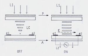
In this case, both linear polarizing filters P and A have their axes of transmission in the same direction. To obtain the 90 degree twisted nematic structure of the LC layer between the two glass plates without an applied electric field (OFF state), the inner surfaces of the glass plates are treated to align the bordering LC molecules at a right angle. This molecular structure is practically the same as in TN LCDs. However, the arrangement of the electrodes e1 and e2 is different. Because they are in the same plane and on a single glass plate, they generate an electric field essentially parallel to this plate. The diagram is not to scale: the LC layer is only a few micrometers thick and so is very small compared with the distance between the electrodes.
The LC molecules have a positive dielectric anisotropy and align themselves with their long axis parallel to an applied electrical field. In the OFF state (shown on the left), entering light L1 becomes linearly polarized by polarizer P. The twisted nematic LC layer rotates the polarization axis of the passing light by 90 degrees, so that ideally no light passes through polarizer A. In the ON state, a sufficient voltage is applied between electrodes and a corresponding electrical field E is generated that realigns the LC molecules as shown on the right of the diagram. Here, light L2 can pass through polarizer A.
In practice, other schemes of implementation exist with a different structure of the LC molecules – for example without any twist in the OFF state. As both electrodes are on the same substrate, they take more space than TN matrix electrodes. This also reduces contrast and brightness.[16]
Super-IPS was later introduced with better response times and colour reproduction.[17][unreliable source?]

Advantages
- IPS panels display consistent, accurate color from all viewing angles.[18] A state-of-the-art (2014) comparison of IPS vs. TN panels concerning color consistency under different viewing angles can be seen on the website of Japan Display Inc.[19]
- Unlike TN LCDs, IPS panels do not lighten or show tailing when touched. This is important for touch-screen devices, such as smartphones and tablet computers.[20]
- IPS panels offer clear and razor-sharp images without reflections, a wide viewing range, stable response time and better coloring.[21][16][unreliable source?][22]
Disadvantages
- IPS panels require up to 15% more power than TN panels.[23]
- IPS panels are more expensive to produce than TN panels.
- IPS panels have slower/longer response times than TN panels.[24]
- IPS panels are sometimes vulnerable to a defect called backlight bleeding.
Alternative technologies
Plane to Line Switching (PLS)
Toward the end of 2010 Samsung Electronics introduced Super PLS (Plane-to-Line Switching) with the intent of providing an alternative to the popular IPS technology which is primarily manufactured by LG Display. It is an "IPS-type" panel technology, and is very similar in performance features, specs and characteristics to LG Display's offering. Samsung adopted PLS panels instead of AMOLED panels, because in the past AMOLED panels had difficulties in realizing full HD resolution on mobile devices. PLS technology was Samsung's wide-viewing angle LCD technology, similar to LG Display's IPS technology.[25]
Samsung asserted the following benefits of Super PLS (commonly referred to as just "PLS") over IPS:[26]
- Further improvement in viewing angle
- 10 percent increase in brightness
- Up to 15 percent decrease in production costs
- Increased image quality
- Flexible panel
Advanced Hyper-Viewing Angle (AHVA)
In 2012 AU Optronics began investment in their own IPS-type technology, dubbed AHVA. This should not be confused with their long standing AMVA technology (which is a VA-type technology). Performance and specs remained very similar to LG Display's IPS and Samsung's PLS offerings. The first 144 Hz compatible IPS-type panels were produced in late 2014 (used first in early 2015) by AUO, beating Samsung and LG Display to providing high refresh rate IPS-type panels.[27][28]
Manufacturers
- AU Optronics
- Acer
- BOE
- Chi Mei Optoelectronics
- Japan Display Inc.
- LG Display (mentioned as largest supplier of IPS LCDs in 2012)[1]
- Newhaven Display
- Panasonic Liquid Crystal Display Co., Ltd
- Samsung Display
- Sony Professional Display
See also
- Computer monitor
- e-paper
- LCD TV
- Liquid-crystal display
- Smart watch
- TFT LCD
References
- ↑ 1.0 1.1 Cross, Jason (18 March 2012). "Digital Displays Explained". TechHive. PC World. p. 4. http://www.techhive.com/article/251988/digital_true_explained.html?page=4.
- ↑ "TFT Technology: Enhancing the viewing angle". Riverdi (TFT Module Manufacturer). https://riverdi.com/technology/#technology-Angle. "However, [twisted nematic] suffers from the phenomenon called gray scale inversion. This means that the display has one viewing side in which the image colors suddenly change after exceeding the specified viewing angle. (see image Inversion Effect)"
- ↑ "Bibliographic data: US3834794 (A) ― 1974-09-10". http://worldwide.espacenet.com/publicationDetails/biblio?locale=en_EP&CC=US&NR=3834794.
- ↑ U.S. Patent 3,834,794: R. Soref, Liquid crystal electric field sensing measurement and display device, filed 28 June 1973.
- ↑ "Bibliographic data: US5576867 (A) ― 1996-11-19". http://worldwide.espacenet.com/publicationDetails/biblio?locale=en_EP&CC=US&NR=5576867.
- ↑ US patent 5576867 patent
- ↑ "2014 SID Honors and Awards". http://informationdisplay.org/IDArchive/2014/MarchApril/HonorsandAwards.aspx.
- ↑ "Espacenet – Bibliographic data". 1997-01-28. http://worldwide.espacenet.com/publicationDetails/biblio?locale=en_EP&CC=US&NR=5598285.
- ↑ U.S. Patent 5,598,285: K. Kondo, H. Terao, H. Abe, M. Ohta, K. Suzuki, T. Sasaki, G. Kawachi, J. Ohwada, Liquid crystal display device, filed Sep 18, 1992 and Jan 20, 1993.
- ↑ "Optical Patterning". Nature. August 22, 1996. http://www.nature.com/nature/journal/v382/n6593/pdf/382666c0.pdf.
- ↑ Technical specifications iPhone 5c
- ↑ Comparison of iPad models
- ↑ IPS-Pro (Evolving IPS technology)
- ↑ "Archived copy". http://www.barco.be/barcoview/downloads/IPS-Pro_LCD_technology.pdf.
- ↑ tech2 News Staff (19 May 2011). "LG Announces Super High Resolution AH-IPS Displays". http://tech.firstpost.com/news-analysis/lg-announces-super-high-resolution-ah-ips-displays-19506.html.
- ↑ 16.0 16.1 Baker, Simon (30 April 2011). "Panel Technologies: TN Film, MVA, PVA and IPS Explained". Tftcentral.co.uk. http://www.tftcentral.co.uk/articles/panel_technologies.htm.
- ↑ "LCD Panel Technology Explained". PChardwarehelp.com. http://www.pchardwarehelp.com/guides/lcd-panel-types.php.
- ↑ Comparisons done by LG Display
- ↑ Visual comparison of IPS and TN done by Japan Display Inc.
- ↑ IPS "Stable Panel"
- ↑ "Panel Mount Monitors | 7 to 27 inches | Beetronics" (in EN-US). https://www.beetronics.com/open-frame-panel-mount-monitors.
- ↑ Mark, Winston (June 30, 2021). "IPS or TN panel?". EsportSource.net. https://www.esportsource.net/monitors/ips-tn-panel/.
- ↑ Ivankov, Alex (1 September 2016). "Advantages and disadvantages of IPS screen technology". http://www.versiondaily.com/advantages-and-disadvantages-of-ips-screen-technology/.
- ↑ "Display and Graphics Guide". The University of Pennsylvania. 3 May 2017. https://www.isc.upenn.edu/how-to/display-and-graphics-guide.
- ↑ "Samsung Adopts IPS instead of AMOLED: Why?". seoul.co.kr. http://www.seoul.co.kr/news/newsView.php?id=20121109023018&spage=1/.
- ↑ "Samsung PLS improves on IPS displays like iPad's, costs less". electronista.com. http://www.electronista.com/articles/10/12/01/samsung.intros.pls.as.improvement.on.lcds/.
- ↑ "AU Optronics develops 144Hz refresh IPS-type display panels". 8 September 2014. http://hexus.net/tech/news/monitors/74389-au-optronics-develops-144hz-refresh-ips-type-display-panels/.
- ↑ "144Hz IPS-type Panels Developed – 1440p as Well". http://www.guru3d.com/news-story/144hz-ips-type-panels-developed-1440p-as-well.html.
External links
de:Flüssigkristallbildschirm#In-Plane Switching (IPS)
