Engineering:Miller effect
In electronics, the Miller effect (named after its discoverer John Milton Miller) accounts for the increase in the equivalent input capacitance of an inverting voltage amplifier due to amplification of the effect of capacitance between the amplifier's input and output terminals, and is given by where is the voltage gain of the inverting amplifier ( positive), and is the feedback capacitance.
Although the term Miller effect normally refers to capacitance, any impedance connected between the input and another node exhibiting gain can modify the amplifier input impedance via this effect. These properties of the Miller effect are generalized in the Miller theorem. The Miller capacitance due to undesired parasitic capacitance between the output and input of active devices like transistors and vacuum tubes is a major factor limiting their gain at high frequencies.
History
When Miller published his work in 1919,[1] he was working on vacuum tube triodes. The same analysis applies to modern devices such as bipolar junction and field-effect transistors.
Derivation

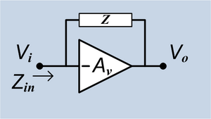
Consider a circuit of an ideal inverting voltage amplifier of gain with an impedance connected between its input and output nodes. The output voltage is therefore . Assuming that the amplifier input draws no current, all of the input current flows through , and is therefore given by
- .
The input impedance of the circuit is
- .
In the Laplace domain (where represents complex frequency), if consists of just a capacitor forming a complex impedance , then the circuit's resulting input impedance will be equivalent to that of a larger capacitance :
- .
This Miller capacitance is the physical capacitance multiplied by the factor .[2]
Effects
As most amplifiers are inverting ( as defined above is positive), the effective capacitance at their inputs is increased due to the Miller effect. This can reduce the bandwidth of the amplifier, restricting its range of operation to lower frequencies. The tiny junction and stray capacitances between the base and collector terminals of a Darlington transistor, for example, may be drastically increased by the Miller effects due to its high gain, lowering the high frequency response of the device.
It is also important to note that the Miller capacitance is the capacitance seen looking into the input. If looking for all of the RC time constants (poles) it is important to include as well the capacitance seen by the output. The capacitance on the output is often neglected since it sees and amplifier outputs are typically low impedance. However if the amplifier has a high impedance output, such as if a gain stage is also the output stage, then this RC can have a significant impact on the performance of the amplifier. This is when pole splitting techniques are used.
The Miller effect may also be exploited to synthesize larger capacitors from smaller ones. One such example is in the stabilization of feedback amplifiers, where the required capacitance may be too large to practically include in the circuit. This may be particularly important in the design of integrated circuits, where capacitors can consume significant area, increasing costs.
Mitigation
The Miller effect may be undesired in many cases, and approaches may be sought to lower its impact. Several such techniques are used in the design of amplifiers.
A current buffer stage may be added at the output to lower the gain between the input and output terminals of the amplifier (though not necessarily the overall gain). For example, a common base may be used as a current buffer at the output of a common emitter stage, forming a cascode. This will typically reduce the Miller effect and increase the bandwidth of the amplifier.
Alternatively, a voltage buffer may be used before the amplifier input, reducing the effective source impedance seen by the input terminals. This lowers the time constant of the circuit and typically increases the bandwidth.
The Miller capacitance can be mitigated by employing neutralisation. This can be achieved by feeding back an additional signal that is in phase opposition to that which is present at the stage output. By feeding back such a signal via a suitable capacitor, the Miller effect can, at least in theory, be eliminated entirely. In practice, variations in the capacitance of individual amplifying devices coupled with other stray capacitances, makes it difficult to design a circuit such that total cancellation occurs. Historically, it was not unknown for the neutralising capacitor to be selected on test to match the amplifying device, particularly with early transistors that had very poor bandwidths. The derivation of the phase inverted signal usually requires an inductive component such as a choke or an inter-stage transformer.
In vacuum tubes, an extra grid (the screen grid) could be inserted between the control grid and the anode. This had the effect of screening the anode from the grid and substantially reducing the capacitance between them. While the technique was initially successful other factors limited the advantage of this technique as the bandwidth of tubes improved. Later tubes had to employ very small grids (the frame grid) to reduce the capacitance to allow the device to operate at frequencies that were impossible with the screen grid.
Impact on frequency response

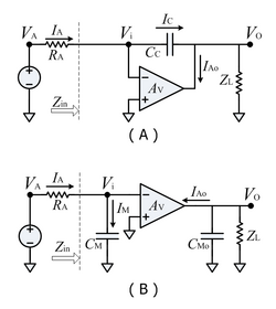
Figure 2A shows an example of Figure 1 where the impedance coupling the input to the output is the coupling capacitor . Thévenin voltage source drives the circuit with Thévenin resistance . The output impedance of the amplifier is considered low enough that the relationship is presumed to hold. At the output, serves as the load. (The load is irrelevant to this discussion: it just provides a path for the current to leave the circuit.) In Figure 2A, the coupling capacitor delivers a current to the output node.
Figure 2B shows a circuit electrically identical to Figure 2A using Miller's theorem. The coupling capacitor is replaced on the input side of the circuit by the Miller capacitance , which draws the same current from the driver as the coupling capacitor in Figure 2A. Therefore, the driver sees exactly the same loading in both circuits. On the output side, the same current from the output as drawn from the coupling capacitor in Figure 2A is instead drawn from a capacitor equal to:
In order for the Miller capacitance to draw the same current in Figure 2B as the coupling capacitor in Figure 2A, the Miller transformation is used to relate to . In this example, this transformation is equivalent to setting the currents equal, that is
or, rearranging this equation
This result is the same as of the Derivation Section.
The present example with frequency independent shows the implications of the Miller effect, and therefore of , upon the frequency response of this circuit, and is typical of the impact of the Miller effect (see, for example, common source). If is 0, the output voltage of the circuit is simply , independent of frequency. However, when is not zero, Figure 2B shows the large Miller capacitance appears at the input of the circuit. The voltage output of the circuit now becomes
and rolls off with frequency once frequency is high enough that ωCMRA ≥ 1. It is a low-pass filter. In analog amplifiers this curtailment of frequency response is a major implication of the Miller effect. In this example, the frequency ω3dB such that ω3dB CMRA = 1 marks the end of the low-frequency response region and sets the bandwidth or cutoff frequency of the amplifier.
The effect of CM upon the amplifier bandwidth is greatly reduced for low impedance drivers (CM RA is small if RA is small). Consequently, one way to minimize the Miller effect upon bandwidth is to use a low-impedance driver, for example, by interposing a voltage follower stage between the driver and the amplifier, which reduces the apparent driver impedance seen by the amplifier.
The output voltage of this simple circuit is always Av vi. However, real amplifiers have output resistance. If the amplifier output resistance is included in the analysis, the output voltage exhibits a more complex frequency response and the impact of the frequency-dependent current source on the output side must be taken into account.[3] Ordinarily these effects show up only at frequencies much higher than the roll-off due to the Miller capacitance, so the analysis presented here is adequate to determine the useful frequency range of an amplifier dominated by the Miller effect.
Miller approximation
This example also assumes Av is frequency independent, but more generally there is frequency dependence of the amplifier contained implicitly in Av. Such frequency dependence of Av also makes the Miller capacitance frequency dependent, so interpretation of CM as a capacitance becomes more difficult. However, ordinarily any frequency dependence of Av arises only at frequencies much higher than the roll-off with frequency caused by the Miller effect, so for frequencies up to the Miller-effect roll-off of the gain, Av is accurately approximated by its low-frequency value. Determination of CM using Av at low frequencies is the so-called Miller approximation.[2] With the Miller approximation, CM becomes frequency independent, and its interpretation as a capacitance at low frequencies is secure.
See also
References and notes
- ↑ John M. Miller, "Dependence of the input impedance of a three-electrode vacuum tube upon the load in the plate circuit," Scientific Papers of the Bureau of Standards, vol.15, no. 351, pages 367-385 (1920). Available on-line at: http://web.mit.edu/klund/www/papers/jmiller.pdf .
- ↑ 2.0 2.1 R.R. Spencer and M.S. Ghausi (2003). Introduction to electronic circuit design.. Upper Saddle River NJ: Prentice Hall/Pearson Education, Inc.. p. 533. ISBN 0-201-36183-3. http://worldcat.org/isbn/0-201-36183-3.
- ↑ See article on pole splitting.
 |
