Engineering:Parasitic capacitance
Parasitic capacitance, or stray capacitance is an unavoidable and usually unwanted capacitance that exists between the parts of an electronic component or circuit simply because of their proximity to each other. When two electrical conductors at different voltages are close together, the electric field between them causes electric charge to be stored on them; this effect is parasitic capacitance. All actual circuit elements such as inductors, diodes, and transistors have internal capacitance, which can cause their behavior to depart from that of 'ideal' circuit elements. Additionally, there is always non-zero capacitance between any two conductors; this can be significant at higher frequencies with closely spaced conductors, such as wires or printed circuit board traces. The parasitic capacitance between the turns of an inductor or other wound component is often described as self-capacitance. However, the term self-capacitance more correctly refers to a different phenomenon; the capacitance of a conductive object without reference to another object.
Description
When two conductors at different potentials are close to one another, they are affected by each other's electric field and store opposite electric charges like a capacitor. Changing the potential v between the conductors requires a current i into or out of the conductors to charge or discharge them.
where C is the capacitance between the conductors. For example, an inductor often acts as though it includes a parallel capacitor, because of its closely spaced windings. When a potential difference exists across the coil, wires lying adjacent to each other are at different potentials. They act like the plates of a capacitor, and store charge. Any change in the voltage across the coil requires extra current to charge and discharge these small 'capacitors'. When the voltage changes only slowly, as in low-frequency circuits, the extra current is usually negligible, but when the voltage changes quickly the extra current is larger and can affect the operation of the circuit.
Coils for high frequencies are often basket-wound to minimise parasitic capacitance.
Effects
At low frequencies parasitic capacitance can usually be ignored, but in high frequency circuits it can be a major problem. In amplifier circuits with extended frequency response, parasitic capacitance between the output and the input can act as a feedback path, causing the circuit to oscillate at high frequency. These unwanted oscillations are called parasitic oscillations.
In high frequency amplifiers, parasitic capacitance can combine with stray inductance such as component leads to form resonant circuits, also leading to parasitic oscillations. In all inductors, the parasitic capacitance will resonate with the inductance at some high frequency to make the inductor self-resonant; this is called the self-resonant frequency. Above this frequency, the inductor actually has capacitive reactance.
The capacitance of the load circuit attached to the output of op amps can reduce their bandwidth. High-frequency circuits require special design techniques such as careful separation of wires and components, guard rings, ground planes, power planes, shielding between input and output, termination of lines, and striplines to minimise the effects of unwanted capacitance.
In closely spaced cables and computer busses, parasitic capacitive coupling can cause crosstalk, which means the signal from one circuit bleeds into another, causing interference and unreliable operation.
Electronic design automation computer programs, which are used to design commercial printed circuit boards, can calculate the parasitic capacitance and other parasitic effects of both components and circuit board traces, and include them in simulations of circuit operation. This is called parasitic extraction.
Miller capacitance
The parasitic capacitance between the input and output electrodes of inverting amplifying devices, such as between the base and collector of transistors, is particularly troublesome because it is multiplied by the gain of the device. This Miller capacitance (first noted in vacuum tubes by John Milton Miller, 1920) is the major factor limiting the high frequency performance of active devices like transistors and vacuum tubes. The screen grid was added to triode vacuum tubes in the 1920s to reduce parasitic capacitance between the control grid and the plate, creating the tetrode, which resulted in a great increase in operating frequency.[1]

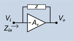
The diagram, right, illustrates how Miller capacitance comes about. Suppose the amplifier shown is an ideal inverting amplifier with voltage gain of A, and Z = C is a capacitance between its input and output. The output voltage of the amplifier is
The current into the input terminal is
So the capacitance at the input of the amplifier is
The input capacitance is multiplied by the gain of the amplifier. This is the Miller capacitance. If the input circuit has an impedance to ground of Ri, then (assuming no other amplifier poles) the output of the amplifier is
The bandwidth of the amplifier is limited by the high frequency roll-off at
So the bandwidth is reduced by the factor (1 + A), approximately the voltage gain of the device. The voltage gain of modern transistors can be 10 - 100 or even higher, so this is a significant limitation.
See also
- Parasitic element (electrical networks)
- Parasitic extraction
References
- ↑ Alley, Charles L.; Atwood, Kenneth W. (1973). Electronic Engineering, 3rd Ed.. New York: John Wiley & Sons.. p. 199. ISBN 0-471-02450-3.
