Engineering:Switching noise jitter
Switching Noise Jitter (SNJ) is the aggregation of variability of noise events in the time-domain on the supply bias of an electronic system, in particular with a voltage regulated supply bias incorporated with closed-loop (feedback) control, for instance, SMPS. SNJ is measurable using real-time spectral histogram analysis[1] and expressed as a rate of occurrence in percentage. The existence of SNJ was firstly demonstrated and termed by TransSiP Inc in 2016 and 2017 at the Applied Power Electronics Conference (APEC),[2] and reviewed with experts at Tektronix prior to be featured as a case study published by Tektronix.[3] The discovery of SNJ was also featured in multiple articles published by Planet Analog magazine[4] and EDN Network.[5] Difficult to filter using conventional LC networks due to variability in both time and frequency domains, SNJ can introduce random errors in analog to digital conversion, affecting both data integrity and system performance in digital communications and location-based services (viz GPS, Satellite positioning)
Creation
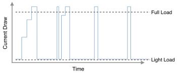
In switching-mode power supplies (SMPS), noise present in the control loop circuitry of the supply causes dislocation in up-slope and down-slope timing of the saw-tooth ripple waveform. As a consequence, the ripple waveform exhibits jitter and noise carried on the ripple also jitters. When this type of supply bias is used to power a system operating in power-saving modes or pulsed applications as shown in Fig. 1 the current drain fluctuates in pulses. Typically a load enters a high power stage (e.g. RX/TX On) for tens of micro- to milli-seconds and is then switched to low power or standby mode for hundreds of milli- or tens of seconds. Inrush currents cause voltage fluctuations due to parasitics of both components and interconnections, creating random noise in addition to the ringing and harmonics normally present. The result is SNJ.
Associated issues
At present, many modern switching DC-DC converters offer dual-mode operation. At full load, the switching frequency is held constant and the voltage is modulated by varying pulse width (pulse-width modulation or PWM), thereby presenting a fixed frequency to the filter circuitry. When light loads are present, PWM efficiencies degrade, so the converter switches to modulation of pulse frequency, typically referred to as pulse-frequency mode (PFM) for increased efficiency. Nevertheless, the dual-mode approach has multiple disadvantages: it creates additional transient noise and momentary fluctuations in output voltage, as well as reduced energy efficiency due to the increased quiescent current required by complex mode-switching circuitry. To make things more difficult, the PFM mode creates a wide spectrum of noise as well as SNJ in the time domain at the output voltage that is difficult to filter.
The SNJ signature, therefore, becomes a dominating influence on the performance of noise-sensitive SoCs,[6] circuit components and fidelity of weak signals after the ripple voltage has been suppressed. In addition, SNJ has a cumulative effect in the analog to digital conversion found in modern digital communications due to the existence of a variety of unwanted noise signals over time which will be digitized and stored in memory.
Time vs. frequency domain

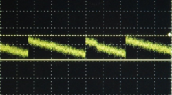
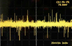
Noise in the output of DC-DC converters may be random or periodic fluctuations in output voltage, analytically expressed as peak-to-peak voltage or noise spectral density. Fig. 2 and Fig. 3 demonstrate the typical visual characteristics of the output from a switching regulator and a linear regulator (also known as "low dropout" or "LDO") respectively. A saw-tooth ripple waveform is the consequence of LC filtering on the output of a switching regulator, while the output of the LDO in this example clearly shows transient/spurious events due to circuit parasitics. These are accompanied by more macro fluctuations in a pulse application due to overshoots and undershoots.
Fig. 4 compares the supply bias noise (ripple) in a GPS application as measured by a spectrum analyzer. The primary bias voltage is provided respectively by a LDO and by a switching regulator. The frequency range of the noise spectrum for both is very similar, lying below 1 MHz. However, the noise amplitude of the LDO is about 20 dB lower than the switching regulator.
So in general practice, the primary bias voltage provided by the LDO is expected to perform better and is generally used as the golden reference when specifying performance characteristics of an active device such as a GPS or wireless communication module or IC, notwithstanding the relatively low DC-DC conversion efficiencies of linear regulators.
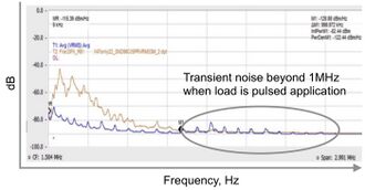
The LDO is indeed able to provide a low-noise bias, but only when the DC load is constant. Of course, in practice the current draw of a load will fluctuate, and careful examinations of the supply bias of pulsed applications will show that transient noise is, in fact, present, as shown in Fig. 5 and this is difficult to filter. Powering a noise-sensitive SoC or circuit component in a pulsed application with an LDO may well turn out to be a sub-optimal solution: in addition to low conversion efficiency, noise is still present on the supply bias in the form of transients which vary in both frequency and density (frequency of occurrence).[7]
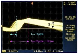
When observed on an oscilloscope, the ripple waveform on the output of a PFM-type DC-DC converter will appear as shown in Fig. 6. Abnormalities occurring in the time-domain increase the "perturbation": the variability of switching events in time relative to a reference. Since the converter is PFM type, the switching frequency changes with the fluctuation of the load. This makes it problematic using frequency-domain measurement to discriminate how much of the variation of the waveform in both timing TON and slope S1 (∆V/∆T) is caused by the response of the controller to the load and how much by the noise in the control loop circuitry.
The waveform in Fig. 7 demonstrates the outcome from the same setup with SNJ conditioning in place: the variability in TON and S1are substantially reduced.
Measurement

Since SNJ occurs on a random basis, the most effective measurement technique employs a determination of how often it occurs. The DPX (digital phosphor)[8] technique from Tektronix[9] is particularly useful, as it directly outputs event density in the form of a histogram analysis. Thanks to the introduction of event density as an additional measurement dimension, a DPX Spectrum display can be used to discriminate between load-induced and jitter-induced movement of the waveform, adding an additional dimension to frequency and amplitude. The color temperature spectrum (“Z” axis) shows the number of occurrences of signals (or ‘event density’) over a set period of time. Z-axis scaling adjustments for maximum and minimum occurrence values can be manipulated to discriminate visually between different signals beneath the maximum amplitude.
Fig. 8 shows the DPX plot of the supply bias waveform shown in Fig. 6. A measurement box, defined by the horizontal frequency and vertical amplitude ranges, is used to define and measure the average event density over a period of time. The distortion of the intermediate (green/yellow) bands on the bitmap is clearly visible.

In this example, the measurement period is set to infinite (i.e. the system collects SNJ continuously on the DPX display until stop). This measurement technique enables the identification and measurement of SNJ in the SMPS output both qualitatively and quantitatively.
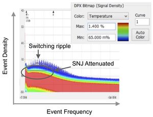
The crucial noise reduction, achieved when the SNJ is conditioned, can be seen clearly in Fig 9. SNJ conditioning has reduced the event density by about 50%. This level of reduction has been shown in field trials to be significant, with demonstrable improvements in device autonomy and performance.
In summary, advances in signal analysis have enabled the discovery of a new component of noise present in electronic systems using DC-DC conversion. Field trials comparing battery-powered devices where SNJ is effectively conditioned to devices using conventional linear regulation and/or switching mode DC-DC conversion have conclusively shown that measurable improvements in performance, precision, and autonomy are obtained.
References
- ↑ Tektronix (June 2016). "Fundamentals of Real-Time Spectral Analysis". https://download.tek.com/document/37W_17249_5_HR_Letter.pdf.
- ↑ https://www.apec-conf.org/about/history/2017-conference-photos/pageindex508/6 [|permanent dead link|dead link}}]
- ↑ "TransSiP Breakthrough into Power Conversion Switching Noise". Tektronix. September 2016. https://www.tek.com/document/case-study/transsip-breakthrough-power-conversion-switching-noise.
- ↑ Taranovich, Steve (6 September 2016). "An Enabling Technology for Power-Constrained Devices". Planet Analog. https://www.planetanalog.com/author.asp?section_id=3065&doc_id=564332.
- ↑ Burr, William; Wong, Desmond (2 September 2016). "Powering wearable electronics: a new dimension". EDN Network. https://www.edn.com/design/power-management/4442645/Powering-Wearable-Electronics--A-New-Dimension.
- ↑ Rahman, M. T.; Forte, D.; Wang, X.; Tehranipoor, M. (December 19–20, 2016). "Enhancing noise sensitivity of embedded SRAMs for robust true random number generation in SoCs". IEEE Asian Hardware-Oriented Security and Trust (AsianHOST). Yilan, Taiwan: IEEE. doi:10.1109/AsianHOST.2016.7835559. ISBN 978-1-5090-5701-6.
- ↑ Wong, Desmond (2013-05-06). "GNSS Receiver Frequency Reference for Successful Satellite Navigation". EDN. https://www.edn.com/design/systems-design/4413426/GNSS-Receiver-Frequency-Reference-for-Successful-Satellite-Navigation. Retrieved 2019-08-07.
- ↑ Guo, Shijian (January 2013). "Design of DPX system for real-time spectrum analysis and signal detection". IEICE Electronics Express. https://www.researchgate.net/publication/275261003.
- ↑ "DPX Overview". 2017-10-12. https://uk.tek.com/dpx-overview.
External links
 |
