Engineering:Low-dropout regulator


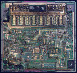
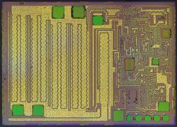
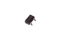
A low-dropout regulator (LDO regulator) is a DC linear voltage regulator that can operate even when the supply voltage is very close to the output voltage.[1] The advantages of an LDO regulator over other DC-to-DC voltage regulators include: the absence of switching noise (in contrast to switching regulators); smaller device size (as neither large inductors nor transformers are needed); and greater design simplicity (usually consists of a reference, an amplifier, and a pass element). The disadvantage is that linear DC regulators must dissipate heat in order to operate.[2]
History
The adjustable low-dropout regulator debuted on April 12, 1977 in an Electronic Design article entitled "Break Loose from Fixed IC Regulators". The article was written by Robert Dobkin, an IC designer then working for National Semiconductor. Because of this, National Semiconductor claims the title of "LDO inventor".[3] Dobkin later left National Semiconductor in 1981 and founded Linear Technology where he was the chief technology officer.[4]
Components

The main components are a power FET and a differential amplifier (error amplifier). One input of the differential amplifier monitors the fraction of the output determined by the resistor ratio of R1 and R2. The second input to the differential amplifier is from a stable voltage reference (bandgap reference). If the output voltage rises too high relative to the reference voltage, the drive to the power FET changes to maintain a constant output voltage.
Regulation
Low-dropout (LDO) regulators operate similarly to all linear voltage regulators. The main difference between LDO and non-LDO regulators is their schematic topology. Instead of an emitter follower topology, low-dropout regulators consist of an open collector or open drain topology, where the transistor may be easily driven into saturation with the voltages available to the regulator. This allows the voltage drop from the unregulated voltage to the regulated voltage to be as low as (limited to) the saturation voltage across the transistor.[2]: Appendix A
For the circuit given in the figure to the right, the output voltage is given as:
If a bipolar transistor is used, as opposed to a field-effect transistor or JFET, significant additional power may be lost to control it, whereas non-LDO regulators take that power from voltage drop itself. For high voltages under very low In-Out difference there will be significant power loss in the control circuit.[5]
Because the power control element is an inverter, another inverting amplifier is required to control it, increasing schematic complexity compared to simple linear regulator.[citation needed]
Power FETs may be preferable in order to reduce power consumption, yet this poses problems when the regulator is used for low input voltage, since FETs usually require 5 to 10 V to close completely. Power FETs may also increase the cost.
Efficiency and heat dissipation
The power dissipated in the pass element and internal circuitry () of a typical LDO is calculated as follows:
where is the quiescent current required by the LDO for its internal circuitry.
Therefore, one can calculate the efficiency as follows:
where
However, when the LDO is in full operation (i.e., supplying current to the load) generally: . This allows us to reduce to the following:
which further reduces the efficiency equation to:
It is important to keep thermal considerations in mind when using a low drop-out linear regulator. Having high current and/or a wide differential between input and output voltage could lead to large power dissipation. Additionally, efficiency will suffer as the differential widens. Depending on the package, excessive power dissipation could damage the LDO or cause it to go into thermal shutdown.
Quiescent current
Among other important characteristics of a linear regulator is the quiescent current, also known as ground current or supply current, which accounts for the difference, although small, between the input and output currents of the LDO, that is:
Quiescent current is current drawn by the LDO in order to control its internal circuitry for proper operation. The series pass element, topologies, and ambient temperature are the primary contributors to quiescent current.[6]
Many applications do not require an LDO to be in full operation all of the time (i.e. supplying current to the load). In this idle state the LDO still draws a small amount of quiescent current in order to keep the internal circuitry ready in case a load is presented. When no current is being supplied to the load, can be found as follows:
Filtering

In addition to regulating voltage, LDOs can also be used as filters. This is especially useful when a system is using switchers, which introduce a ripple in the output voltage occurring at the switching frequency. Left alone, this ripple has the potential to adversely affect the performance of oscillators,[7] data converters,[8] and RF systems[9] being powered by the switcher. However, any power source, not just switchers, can contain AC elements that may be undesirable for design.
Two specifications that should be considered when using an LDO as a filter are power supply rejection ratio (PSRR) and output noise.
Specifications
An LDO is characterized by its drop-out voltage, quiescent current, load regulation, line regulation, maximum current (which is decided by the size of the pass transistor), speed (how fast it can respond as the load varies), voltage variations in the output because of sudden transients in the load current, output capacitor and its equivalent series resistance.[10] Speed is indicated by the rise time of the current at the output as it varies from 0 mA load current (no load) to the maximum load current. This is basically decided by the bandwidth of the error amplifier. It is also expected from an LDO to provide a quiet and stable output in all circumstances (example of possible perturbation could be: sudden change of the input voltage or output current). Stability analysis put in place some performance metrics to get such a behaviour and involve placing poles and zeros appropriately. Most of the time, there is a dominant pole that arise at low frequencies while other poles and zeros are pushed at high frequencies.
Power supply rejection ratio
PSRR refers to the LDO's ability to reject ripple it sees at its input.[11] As part of its regulation, the error amplifier and bandgap attenuate any spikes in the input voltage that deviate from the internal reference to which it is compared.[12] In an ideal LDO, the output voltage would be solely composed of the DC frequency. However, the error amplifier is limited in its ability to gain small spikes at high frequencies. PSRR is expressed as follows:[11]
As an example, an LDO that has a PSRR of 55 dB at 1 MHz attenuates a 1 mV input ripple at this frequency to just 1.78 µV at the output. A 6 dB increase in PSRR roughly equates to an increase in attenuation by a factor of 2.
Most LDOs have relatively high PSRR at lower frequencies (10 Hz – 1 kHz). However, a Performance LDO is distinguished in having high PSRR over a broad frequency spectrum (10 Hz – 5 MHz). Having high PSRR over a wide band allows the LDO to reject high-frequency noise like that arising from a switcher. Similar to other specifications, PSRR fluctuates over frequency, temperature, current, output voltage, and the voltage differential.
Output noise
The noise from the LDO itself must also be considered in filter design. Like other electronic devices, LDOs are affected by thermal noise, bipolar shot noise, and flicker noise.[9] Each of these phenomena contribute noise to the output voltage, mostly concentrated over the lower end of the frequency spectrum. In order to properly filter AC frequencies, an LDO must both reject ripple at the input while introducing minimal noise at the output. Efforts to attenuate ripple from the input voltage could be in vain if a noisy LDO just adds that noise back again at the output.
Load regulation
Load regulation is a measure of the circuit's ability to maintain the specified output voltage under varying load conditions. Load regulation is defined as:
The worst case of the output voltage variations occurs as the load current transitions from zero to its maximum rated value or vice versa.[6]
Line regulation
Line regulation is a measure of the circuit's ability to maintain the specified output voltage with varying input voltage. Line regulation is defined as:
Like load regulation, line regulation is a steady state parameter—all frequency components are neglected. Increasing DC open-loop current gain improves the line regulation.[6]
Transient response
The transient response is the maximum allowable output voltage variation for a load current step change. The transient response is a function of the output capacitor value (), the equivalent series resistance (ESR) of the output capacitor, the bypass capacitor () that is usually added to the output capacitor to improve the load transient response, and the maximum load-current (). The maximum transient voltage variation is defined as follows:
Where corresponds to the closed-loop bandwidth of an LDO regulator. is the voltage variation resulting from the presence of the ESR () of the output capacitor. The application determines how low this value should be.
Evolution and the future
A competitor to the LDO, the IVR (integrated voltage regulator) appears to offer solutions to many of the issues with efficiency and performance that LDO regulators suffer. IVRs combine a switching voltage regulator with all necessary control circuitry into a single device which results in a 10x size reduction and 10-50% energy savings.[13]
See also
- Linear regulator
- Low-voltage detect (sometimes confused with LDO regulator}
- Voltage regulator
- Switched-mode power supply
- List of linear integrated circuits
- LM7805
References
- ↑ Paul Horowitz and Winfield Hill (1989). The Art of Electronics. Cambridge University Press. pp. 343–349. ISBN 978-0-521-37095-0. https://books.google.com/books?id=bkOMDgwFA28C&q=low-dropout&pg=PA343.
- ↑ 2.0 2.1 Jim Williams (March 1, 1989). "High Efficiency Linear Regulators". Linear Technology. http://www.linear.com/docs/4126.
- ↑ Low Dropout Regulators, Linear Regulators, CMOS Linear Regulator
- ↑ Don Tuite (September 1, 2007). "Inventor Updates A Classic 30 Years Later". http://electronicdesign.com/Articles/Index.cfm?ArticleID=16406.
- ↑ Simpson, Chester. "Linear and Switching Voltage Regulator Fundamentals". Texas Instruments. http://www.ti.com/lit/snva558.
- ↑ 6.0 6.1 6.2 6.3 Lee, Bang S.. "Understanding the Terms and Definitions of LDO Voltage Regulators". Texas Instruments. http://www.ti.com/lit/slva079.
- ↑ Mohammed, Habeeb. "Supply Noise Effect on Oscillator Phase Noise". http://www.ti.com/lit/slwa066.
- ↑ Ramus, Xavier. "Measuring PSR in an ADC". https://e2e.ti.com/blogs_/b/powerhouse/archive/2015/01/24/measuring-psrr-in-an-adc.
- ↑ 9.0 9.1 Pithadia, Sanjay. "LDO Noise Demystified". Texas Instruments. http://www.ti.com/lit/slaa412.
- ↑ Current Efficient, Low Voltage LDO A Thesis by Rincon-Mora
- ↑ 11.0 11.1 Pithadia, Sanjay. "LDO PSRR Measurement Simplified". Texas Instruments. http://www.ti.com/lit/slaa414.
- ↑ Day, Michael. "Understanding Low Drop Out (LDO) Regulators". Texas Instruments. http://www.ti.com/lit/slup239.
- ↑ "What is an IVR?". Empower Semiconductor. https://www.empowersemi.com/product-page-ivr/.
External links
- Understanding Low Dropout Regulators - Basics
- Understanding LDO Regulators - TI
- Understanding Noise and PSRR in LDOs - All About Circuits
- Understanding Noise in LDOs - TI
- Index of TI LDO Application Notes - TI
 |
