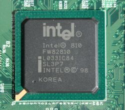
Intel 810

The Intel 810 chipset was released by Intel in early 1999 with the code-name "Whitney"[1] as a platform for the P6-based Socket 370 CPU series, including the Pentium III and Celeron processors. Some motherboard designs include Slot 1 for older Intel CPUs or a combination of both Socket 370 and Slot 1. It targeted the low-cost segment of the market, offering a robust platform for uniprocessor budget systems with integrated graphics. The 810 was Intel's first chipset design to incorporate a hub architecture which was claimed to have better I/O throughput[2] and an integrated GPU, derived from the Intel740.[3]
Overview
There are 5 variants of the 810:
- 810-L: microATX (4 PCI), no display cache, ATA33 hard disk interface.
- 810: microATX (4 PCI), no display cache, ATA33 and ATA66.
- 810-DC100: ATX (6 PCI), 4 MB display cache (AIMM), ATA33 and ATA66.
- 810E: added support for 133MHz FSB, Pentium III or Celeron "Coppermine-EB" Series CPU.
- 810E2:added support for Pentium III and Celeron CPUs with 130 nm "Tualatin" core, ATA100 and 4 USB 1.1 ports.
Intel 810 attempted to integrate as much functionality into the motherboard as possible. Features include:[2][4]
- 66 and 100 MHz bus support
- 2 USB ports
- An integrated graphics processor.
- Based upon the Intel740 2D/3D accelerator (i752).
- Optional dedicated video RAM cache or use of system RAM.
- Hardware motion compensation for DVD playback.
- Digital video output
- AC'97 modem and audio
The hub design consisted of 3 chips, including the Graphics & Memory Controller Hub (GMCH), I/O Controller Hub (ICH), and the Firmware Hub (FWH). These components are connected by a separate 266 MB/s bus, double the previously typical 133 MB/s attachment via PCI-Bus. The added bandwidth was necessary because of increasing demands data transfer between components.[4]
The early GMCH (82810) chips (A2 stepping; S-spec numbers can be found on the fourth line of the chipset: SL35K, SL35X, SL3KK, SL3KL, Q790, Q789) could only support Celeron processors as they were unable to handle SSE instructions correctly.
810 supports asynchronous bus clock operation between the chipset and CPU (front side bus) and the system RAM. So, if the machine is equipped with a Celeron that uses only a 66 MHz bus, PC100 SDRAM can still be taken advantage of and will benefit the IGP.[4]
Boards based on the chipset do not have an AGP expansion slot, leaving the user to make do with PCI for video card options. 810-based boards include an AMR expansion slot. Additionally, the integrated graphics does not support 32-bit graphics mode, forcing the user to downsample the 810's standard 24-bit mode to 16-bit in order to run most games or full screen DirectX/OpenGL programs; many games will automatically downsample the output to 16-bit upon loading, however others will simply exit with or without an error or even crash due to the 24-bit mode not being supported by the game. The onboard graphics' performance in games was also unsatisfactory, and many games of that time had to be run at low resolution and low detail levels to be playable.
See also
- List of Intel chipsets
- P6 microarchitecture
References
- ↑ Shimpi, Anand Lal. "Intel 800 Chipset". http://www.anandtech.com/show/299.
- ↑ 2.0 2.1 Intel 810, Intel.com, accessed March 12, 2007.
- ↑ "Evolution of Intel Graphics: I740 to Iris Pro". 4 February 2017. https://www.tomshardware.com/amp/picturestory/693-intel-graphics-evolution.html.
- ↑ 4.0 4.1 4.2 Intel 810 Chipset Review, X-bit Labs, May 25, 1999.
 |
