Microsecond Bus

The Microsecond Bus, μSB or MSB is an asymmetric serial communication interface specification for short-distance communication between a master and multiple slaves. The MSB has been developed in the first place for motor management applications in order to reduce the classical pulse-width modulation (PWM) of power loads by a fast serial interface with low pin count and low latency for the downstream to the smart power device. The downstream from master to slave is synchronous with low latency, while the upstream, mainly used to send diagnostic information from the slave back to the master is asynchronous, and can be slower.
The name of the bus originates from the time of one microsecond to transmit 16 bits in one of the first implementations. The bus was developed by Infineon and published in SAE International in 2005.[1] In the meantime the bus has been adopted by several other automotive semiconductor providers.
Interface

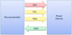
The MSC downlink specifies:
- FCL : Serial Clock (output from master).
- FDA : Master Output, Slave Input (output from master).
- SSY : Slave Select (active low, output from master).
In case of LVDS signaling FDA and FCL are split into four differential lines.
Comparison with SPI
The clocking scheme of the fast synchronous downstream is closely related to the scheme of the SPI bus. There are implementations for single-ended TTL level signaling, as well as LVDS signalling. The (optional) upstream is asynchronous to the downstream clock and can be slowed down by a variable clock division of the downstream clock.
See also
References
- ↑ N Kelling, M König, K McNair, Microsecond Bus, SAE, 2005, http://papers.sae.org/2005-01-0057/
 |
