Physics:A15 phases

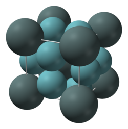
The A15 phases (also known as β-W or Cr3Si structure types) are series of intermetallic compounds with the chemical formula A3B (where A is a transition metal and B can be any element) and a specific structure. The A15 phase is also one of the members in the Frank–Kasper phases family.[1] Many of these compounds have superconductivity at around 20 K (−253 °C; −424 °F), which is comparatively high, and remain superconductive in magnetic fields of tens of teslas (hundreds of kilogauss). This kind of superconductivity (Type-II superconductivity) is an important area of study as it has several practical applications.
History
The first time that A15 structure was observed was in 1931 when an electrolytically deposited layer of tungsten was examined.[2] Discussion of whether the β-tungsten structure is an allotrope of tungsten or the structure of a tungsten suboxide was long-standing, but since the 1950s there has been many publications showing that the material is a true allotrope of tungsten.[3][4][5][6][7][8]
The first intermetallic compound discovered with typical A3B composition was chromium silicide Cr3Si, discovered in 1933.[9] Several other compounds with A15 structure were discovered in following years. No large interest existed in research on those compounds. This changed with the discovery that vanadium silicide V3Si showed superconductivity at around 17 K in 1953.[10] In following years, several other A3B superconductors were found.[11] Niobium-germanium held the record for the highest temperature of 23.2 K from 1973 until the discovery of the cuprate superconductors in 1986. It took time for the method to produce wires from the very brittle A15 phase materials to be established. This method is still complicated. Though some A15 phase materials can withstand higher magnetic field intensity and have higher critical temperatures than the NbZr and NbTi alloys, NbTi is still used for most applications due to easier manufacturing.[12] Nb3Sn is used for some high field applications, for example high-end MRI scanners and NMR spectrometers.
A relaxed form of the Voronoi diagram of the A15 phase seems to have the least surface area among all the possible partitions of three-dimensional Euclidean space in regions of equal volume.[citation needed] This partition, also known as the Weaire–Phelan structure, is often present in clathrate hydrates.
Examples
- Vanadium-silicon
- Vanadium-gallium
- Niobium-germanium
- Niobium-tin
- Titanium-gold
- Tungsten (β-phase)
See also
- Weaire–Phelan structure, for the space tessellation generated by A15 phases
References
- ↑ Frank, F. C.; Kasper, J. S. (1959-07-10). "Complex alloy structures regarded as sphere packings. II. Analysis and classification of representative structures" (in en). Acta Crystallographica 12 (7): 483–499. doi:10.1107/S0365110X59001499. ISSN 0365-110X. http://scripts.iucr.org/cgi-bin/paper?S0365110X59001499.
- ↑ Hartmann, Hellmuth; Ebert, Fritz; Bretschneider, Otto (1931). "Elektrolysen in Phosphatschmelzen. I. Die elektrolytische Gewinnung von α- und β-Wolfram". Zeitschrift für anorganische und allgemeine Chemie 198: 116–140. doi:10.1002/zaac.19311980111.
- ↑ Liu, Jiaxing; Barmak, Katayun (2016-02-01). "Topologically close-packed phases: Deposition and formation mechanism of metastable β-W in thin films" (in en). Acta Materialia 104: 223–227. doi:10.1016/j.actamat.2015.11.049. ISSN 1359-6454. Bibcode: 2016AcMat.104..223L.
- ↑ Weerasekera, I. A.; Shah, S. Ismat; Baxter, David V.; Unruh, K. M. (1994-06-13). "Structure and stability of sputter deposited beta‐tungsten thin films". Applied Physics Letters 64 (24): 3231–3233. doi:10.1063/1.111318. ISSN 0003-6951. Bibcode: 1994ApPhL..64.3231W. https://aip.scitation.org/doi/abs/10.1063/1.111318.
- ↑ O’Keefe, M. J.; Grant, J. T. (1996-06-15). "Phase transformation of sputter deposited tungsten thin films with A‐15 structure". Journal of Applied Physics 79 (12): 9134–9141. doi:10.1063/1.362584. ISSN 0021-8979. Bibcode: 1996JAP....79.9134O. https://aip.scitation.org/doi/abs/10.1063/1.362584.
- ↑ Kiss, A. B. (1998). "Thermoanalytical Study of the Composition of β-tungsten". Journal of Thermal Analysis and Calorimetry 54 (3): 815–824. doi:10.1023/A:1010143904328.
- ↑ Petroff, P.; Sheng, T. T.; Sinha, A. K.; Rozgonyi, G. A.; Alexander, F. B. (June 1973). "Microstructure, growth, resistivity, and stresses in thin tungsten films deposited by rf sputtering". Journal of Applied Physics 44 (6): 2545–2554. doi:10.1063/1.1662611. ISSN 0021-8979. Bibcode: 1973JAP....44.2545P. http://dx.doi.org/10.1063/1.1662611.
- ↑ Mannella, G.; Hougen, J. O. (August 1956). ""β-Tungsten" as a Product of Oxide Reduction" (in en). The Journal of Physical Chemistry 60 (8): 1148–1149. doi:10.1021/j150542a035. ISSN 0022-3654. https://pubs.acs.org/doi/abs/10.1021/j150542a035.
- ↑ Boren, B. (1933). "X-Ray Investigation of Alloys of Silicon with Chromium, Manganese, Cobalt and Nickel". Ark. Kern., Min. Geol 11A (10): 2–10.
- ↑ Hardy, George; Hulm, John (1953). "Superconducting Silicides and Germanides". Physical Review 89 (4): 884. doi:10.1103/PhysRev.89.884. Bibcode: 1953PhRv...89Q.884H.
- ↑ Izyumov, Yurii A; Kurmaev, Z Z (1974). "Physical properties and electronic structure of superconducting compounds with theβ-tungsten structure". Soviet Physics Uspekhi 17 (3): 356. doi:10.1070/PU1974v017n03ABEH004136. Bibcode: 1974SvPhU..17..356I.
- ↑ Sheahen, Thomas P (1994). Introduction to high-temperature superconductivity. Springer. p. 32. ISBN 978-0-306-44793-8. https://books.google.com/books?id=dRhQZBqjT14C&pg=PA32.
Further reading
- Graef, Marc De; McHenry, Michael E (2007). Structure of materials: an introduction to crystallography, diffraction and symmetry. Cambridge University Press. pp. 518–521. ISBN 978-0-521-65151-6. https://books.google.com/books?id=nJHSqEseuIUC&pg=PA518.
- Sauthoff, G (1995). Intermetallics. Wiley. pp. 95–97. ISBN 978-3-527-29320-9. https://books.google.com/books?id=ORV48cYEPMYC&pg=PA95.
 |
