Engineering:Back end of line


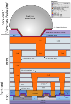
The back end of line (BEOL) is the second portion of IC fabrication where the individual devices (transistors, capacitors, resistors, etc.) get interconnected with wiring on the wafer, the metalization layer. Common metals are copper and aluminum.[1] BEOL generally begins when the first layer of metal is deposited on the wafer. BEOL includes contacts, insulating layers (dielectrics), metal levels, and bonding sites for chip-to-package connections.
After the last FEOL step, there is a wafer with isolated transistors (without any wires). In BEOL part of fabrication stage contacts (pads), interconnect wires, vias and dielectric structures are formed. For modern IC process, more than 10 metal layers can be added in the BEOL.
Steps of the BEOL:
- Silicidation of source and drain regions and the polysilicon region.
- Adding a dielectric (first, lower layer is pre-metal dielectric (PMD) – to isolate metal from silicon and polysilicon), CMP processing it
- Make holes in PMD, make a contacts in them.
- Add metal layer 1
- Add a second dielectric, called the inter-metal dielectric (IMD)
- Make vias through dielectric to connect lower metal with higher metal. Vias filled by Metal CVD process.
- Repeat steps 4–6 to get all metal layers.
- Add final passivation layer to protect the microchip
Before 1998, practically all chips used aluminium for the metal interconnection layers.[2]
The four metals with the highest electrical conductivity are silver with the highest conductivity, then copper, then gold, then aluminium.[citation needed]
After BEOL there is a "back-end process" (also called post-fab), which is done not in the cleanroom, often by a different company. It includes wafer test, wafer backgrinding, die separation, die tests, IC packaging and final test.
See also
References
- ↑ Karen A. Reinhardt and Werner Kern (2008). Handbook of Silicon Wafer Cleaning Technology (2nd ed.). William Andrew. p. 202. ISBN 978-0-8155-1554-8. https://books.google.com/books?id=UPaD8JUCKr0C&pg=PA202.
- ↑ "Copper Interconnect Architecture". http://www.pctechguide.com/cpu-architecture/copper-interconnect-architecture.
Further reading
- "Chapter 11: Back End Technology". Silicon VLSI Technology: Fundamentals, Practice, and Modeling. Prentice Hall. 2000. pp. 681–786. ISBN 0-13-085037-3. https://archive.org/details/siliconvlsitechn00plum.
- "Chapter 7.2.2: CMOS Process Integration: Backend-of-the-line Integration". CMOS: Circuit Design, Layout, and Simulation. Wiley-IEEE. 2010. pp. 199–208 [177–79]. ISBN 978-0-470-88132-3. https://books.google.com/books?id=N0XgLh2d2pkC.
 |

