Engineering:MIS capacitor
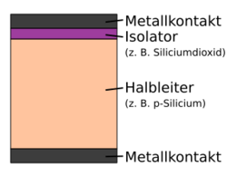
A MIS capacitor is a capacitor formed from a layer of metal, a layer of insulating material and a layer of semiconductor material. It gets its name from the initials of the metal-insulator-semiconductor structure. As with the MOS field-effect transistor structure, for historical reasons, this layer is also often referred to as a MOS capacitor, but this specifically refers to an oxide insulator material.
The maximum capacitance, CMIS(max) is calculated analogously to the plate capacitor:
- [math]\displaystyle{ C_\mathrm{MIS(max)}=\varepsilon_0\varepsilon_r \cdot { {A} \over {d} } }[/math]
where :
- εr is the insulator's relative permittivity
- ε0 is the permittivity of the vacuum
- A is the area
- d is the insulator thickness
The production method depends on materials used (it is even possible that polymers can be used as the insulator). We will consider an example of a MOS capacitor based on silicon and silicon dioxide. On the semiconductor substrate, a thin layer of oxide (silicon dioxide) is applied (by, for example, thermal oxidation, or chemical vapour deposition) and then coated with a metal.
This structure and thus a capacitor of this type is present in every MIS field-effect transistor, such as MOSFETs. For the steady reduction of the size of structures in microelectronics, the following facts are clear. From the formula above it follows that capacitance increases with ever thinner layers of insulation. For all MIS devices the insulation thickness cannot fall below a minimum of around 10 nm. Using thinner insulation than this leads to the occurrence of tunneling through the insulating material (dielectric). Due to this, the use of so-called high-κ materials as the insulator material is being investigated (as of 2009).
This article does not cite any external source. HandWiki requires at least one external source. See citing external sources. (2021) (Learn how and when to remove this template message) |
 |


